C8051F800DK Silicon Laboratories Inc, C8051F800DK Datasheet - Page 12
C8051F800DK
Manufacturer Part Number
C8051F800DK
Description
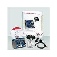
KIT DEV C8051F800
Manufacturer
Silicon Laboratories Inc
Type
MCUr
Specifications of C8051F800DK
Contents
Board, Cables, CD, Debugger, Power Supply
Processor To Be Evaluated
C8051F800
Data Bus Width
16 bit
Interface Type
USB
Operating Supply Voltage
7 V to 15 V
Lead Free Status / RoHS Status
Contains lead / RoHS non-compliant
For Use With/related Products
C8051F8xx
Lead Free Status / Rohs Status
Supplier Unconfirmed
Other names
336-1797


C8051F800-DK
7.4. Switches and LEDs (J3)
Two push-button switches are provided on the target board. The switch labeled ‘RESET’ (SW1 in schematic) is
connected to the reset pin (RST) of the C8051F800. Pressing this switch puts the device into its hardware-reset
state. The switch labeled “P1.4” (SW2 in schematic) is connected to the C8051F800’s general purpose I/O (GPIO)
pin through headers. Pressing this switch generates a logic low signal on the port pin. Remove the shorting block
from the header to disconnect this switch from the port pin. The port pin signal is also routed to a pin on the J1 I/O
connector. See Table 1 for the port pins and headers corresponding to each switch.
Two capacitive sense switches are also provided on the target board. The operation of these switches needs
appropriate code running on the C8051F800 MCU that can sense the state of the switch. Note that no shorting
blocks should be present on J3[15-16] and J3[17-18] for proper operation of these switches. See Section 6.3.
"Capacitive Sense Switch Example‚" on page 8 for details about example source code.
Six LEDs are provided on the target board to serve as indicators. The red LED labeled “PWR” is used to indicate
the presence of power to the target board. Another red LED labeled “USB” is used to indicate a valid USB
connection via the USB connector labeled “COMM.” Note that this LED will light up only after CP210x device
drivers are loaded successfully on the PC. The four green LEDs labeled with port pin names P1.0_LED through
P1.3_LED are connected to the C8051F800’s GPIO pins P1.0 through P1.3, respectively, via the header J3.
Remove the shorting block from the header to disconnect the LED from the port pin. The port pin signal is also
routed to a pin on the J1 I/O connector. See Table 1 for the port pins and headers corresponding to each LED.
12
*Note: Shorting blocks should NOT be present at these headers for
P1.5 (Capacitive Sense)
P1.6 (Capacitive Sense)
P1.0_LED (Green LED)
P1.1_LED (Green LED)
P1.2_LED (Green LED)
P1.3_LED (Green LED)
PWR (Red LED)
USB (Red LED)
RESET (SW1)
Description
the proper operation of the capacitive sense switches.
P1.4 (SW2)
Table 1. Target Board I/O Descriptions
Rev. 0.1
USB Active
Power
Reset
P1.4
P1.0
P1.1
P1.2
P1.3
P1.5
P1.6
I/O
Header(s)
J3[15-16]*
J3[17-18]*
J3[9-10]
J3[1-2]
J3[3-4]
J3[5-6]
J3[7-8]
none
none
none
Related parts for C8051F800DK
Image
Part Number
Description
Manufacturer
Datasheet
Request
R

Part Number:
Description:
SMD/C°/SINGLE-ENDED OUTPUT SILICON OSCILLATOR
Manufacturer:
Silicon Laboratories Inc
Part Number:
Description:
Manufacturer:
Silicon Laboratories Inc
Datasheet:
Part Number:
Description:
N/A N/A/SI4010 AES KEYFOB DEMO WITH LCD RX
Manufacturer:
Silicon Laboratories Inc
Datasheet:
Part Number:
Description:
N/A N/A/SI4010 SIMPLIFIED KEY FOB DEMO WITH LED RX
Manufacturer:
Silicon Laboratories Inc
Datasheet:
Part Number:
Description:
N/A/-40 TO 85 OC/EZLINK MODULE; F930/4432 HIGH BAND (REV E/B1)
Manufacturer:
Silicon Laboratories Inc
Part Number:
Description:
EZLink Module; F930/4432 Low Band (rev e/B1)
Manufacturer:
Silicon Laboratories Inc
Part Number:
Description:
I°/4460 10 DBM RADIO TEST CARD 434 MHZ
Manufacturer:
Silicon Laboratories Inc
Part Number:
Description:
I°/4461 14 DBM RADIO TEST CARD 868 MHZ
Manufacturer:
Silicon Laboratories Inc
Part Number:
Description:
I°/4463 20 DBM RFSWITCH RADIO TEST CARD 460 MHZ
Manufacturer:
Silicon Laboratories Inc
Part Number:
Description:
I°/4463 20 DBM RADIO TEST CARD 868 MHZ
Manufacturer:
Silicon Laboratories Inc
Part Number:
Description:
I°/4463 27 DBM RADIO TEST CARD 868 MHZ
Manufacturer:
Silicon Laboratories Inc
Part Number:
Description:
I°/4463 SKYWORKS 30 DBM RADIO TEST CARD 915 MHZ
Manufacturer:
Silicon Laboratories Inc
Part Number:
Description:
N/A N/A/-40 TO 85 OC/4463 RFMD 30 DBM RADIO TEST CARD 915 MHZ
Manufacturer:
Silicon Laboratories Inc
Part Number:
Description:
I°/4463 20 DBM RADIO TEST CARD 169 MHZ
Manufacturer:
Silicon Laboratories Inc