C8051T630DK Silicon Laboratories Inc, C8051T630DK Datasheet - Page 7
C8051T630DK
Manufacturer Part Number
C8051T630DK
Description
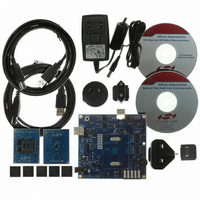
KIT DEV FOR C8051T630 FAMILY
Manufacturer
Silicon Laboratories Inc
Type
MCUr
Specifications of C8051T630DK
Contents
Board, daughter boards, power adapter, cables, documentation and software
Processor To Be Evaluated
C8051T63x
Interface Type
USB
Lead Free Status / RoHS Status
Lead free / RoHS Compliant
For Use With/related Products
C8051T630, T631, T632, T633, T634 and T635 MCUs
For Use With
336-1465 - BOARD SOCKET DAUGHTER 20-QFN
Lead Free Status / Rohs Status
Lead free / RoHS Compliant
Other names
336-1464


6. Example Source Code
Example source code and register definition files are provided by default in the SiLabs\MCU\Examples\C8051T63x
directory during IDE installation. These files may be used as a template for code development.
6.1. Register Definition Files
Register definition files C8051T630.inc, C8051T630_defs.h, and compiler_defs.h, define all SFR registers and bit
addressable control/status bits. They are installed by default into the SiLabs\MCU\Examples\C8051T63x directory
during IDE installation. The register and bit names are identical to those used in the C8051T63x data sheet. The
register definition files are also installed in the default search path used by the Keil Software 8051 tools. Therefore,
when using the Keil 8051 tools included with the development kit (A51, C51), it is not necessary to copy a register
definition file to each project's file directory.
6.2. Blinking LED Example
The example source files T63x_Blinky.asm and T63x_Blinky.c show examples of several basic C8051T63x
functions. These include disabling the watchdog timer (WDT), configuring the Port I/O crossbar, configuring a timer
for an interrupt routine, initializing the system clock, and configuring a GPIO port. When compiled/assembled and
linked, these programs flash the green LED on the C8051T630 Motherboard about ten times a second using the
interrupt handler with a timer.
7. Development Boards
The C8051T63x Development Kit includes a motherboard that interfaces to various daughter boards. The
C8051T630 Emulation Daughter Board contains a C8051F336 device to be used for preliminary software
development. The C8051T630 Socket Daughter Board allows programming and evaluation of the actual
C8051T63x family of devices. Numerous input/output (I/O) connections are provided on the motherboard to
facilitate prototyping. Figure 3 shows the C8051T630 Motherboard and indicates locations for various I/O
connectors. Figure 4 shows the factory default shorting block positions. Figures 5 and 6 show the available
C8051T630 daughter boards.
P1, P2
P3
P4
P5
J1
J2
J3
J4
J5
J6
J7
J8
J9
J10
J11
J12
J13
Daughter board connection
Power connector that accepts input from 7.5 V dc to 15 V dc unregulated power adapter
USB connector for UART to USB communications interface
USB Debug interface connector
Analog I/O terminal block
Port 0 header
Port 1 header
Port 2 header
Connects P0.1 (IDAC) pin to grounded resistor to produce voltage output at IDAC pin.
Power supply selection header (See “7.3. Power Supply Headers (J6 and J7)”)
Power supply enable header that connects power source selected on J6 to the board's main
power supply net
Communications interface control signal header
Connects port pin P0.7 to the switch labeled "SW" and port pin P1.3 to the LED labeled "LED"
Communications interface data signal header
VPP supply connection used when programming EPROM devices
Connects potentiometer to the port pin, P1.6
Additional connections to ground
Rev. 0.1
C8051T63x-DK
7
Related parts for C8051T630DK
Image
Part Number
Description
Manufacturer
Datasheet
Request
R

Part Number:
Description:
SMD/C°/SINGLE-ENDED OUTPUT SILICON OSCILLATOR
Manufacturer:
Silicon Laboratories Inc
Part Number:
Description:
Manufacturer:
Silicon Laboratories Inc
Datasheet:
Part Number:
Description:
N/A N/A/SI4010 AES KEYFOB DEMO WITH LCD RX
Manufacturer:
Silicon Laboratories Inc
Datasheet:
Part Number:
Description:
N/A N/A/SI4010 SIMPLIFIED KEY FOB DEMO WITH LED RX
Manufacturer:
Silicon Laboratories Inc
Datasheet:
Part Number:
Description:
N/A/-40 TO 85 OC/EZLINK MODULE; F930/4432 HIGH BAND (REV E/B1)
Manufacturer:
Silicon Laboratories Inc
Part Number:
Description:
EZLink Module; F930/4432 Low Band (rev e/B1)
Manufacturer:
Silicon Laboratories Inc
Part Number:
Description:
I°/4460 10 DBM RADIO TEST CARD 434 MHZ
Manufacturer:
Silicon Laboratories Inc
Part Number:
Description:
I°/4461 14 DBM RADIO TEST CARD 868 MHZ
Manufacturer:
Silicon Laboratories Inc
Part Number:
Description:
I°/4463 20 DBM RFSWITCH RADIO TEST CARD 460 MHZ
Manufacturer:
Silicon Laboratories Inc
Part Number:
Description:
I°/4463 20 DBM RADIO TEST CARD 868 MHZ
Manufacturer:
Silicon Laboratories Inc
Part Number:
Description:
I°/4463 27 DBM RADIO TEST CARD 868 MHZ
Manufacturer:
Silicon Laboratories Inc
Part Number:
Description:
I°/4463 SKYWORKS 30 DBM RADIO TEST CARD 915 MHZ
Manufacturer:
Silicon Laboratories Inc
Part Number:
Description:
N/A N/A/-40 TO 85 OC/4463 RFMD 30 DBM RADIO TEST CARD 915 MHZ
Manufacturer:
Silicon Laboratories Inc
Part Number:
Description:
I°/4463 20 DBM RADIO TEST CARD 169 MHZ
Manufacturer:
Silicon Laboratories Inc