CY8CKIT-020 Cypress Semiconductor Corp, CY8CKIT-020 Datasheet - Page 58
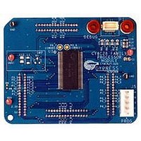
CY8CKIT-020
Manufacturer Part Number
CY8CKIT-020
Description
KIT PSOC CY8C28 FAMILY PROCESSOR
Manufacturer
Cypress Semiconductor Corp
Series
PSoC®r
Type
MCUr
Specifications of CY8CKIT-020
Contents
Board, Software and Documentation
Silicon Manufacturer
Cypress
Core Architecture
PSoC
Features
Programmable System-on-chip Design Methodology And Architecture
Kit Contents
PSoC CY8C28 Module, Doc, CD
Silicon Core Number
CY8C28
Silicon Family Name
PSoC
Rohs Compliant
Yes
Lead Free Status / RoHS Status
Lead free / RoHS Compliant
For Use With/related Products
CY8C28 Family
Lead Free Status / Rohs Status
Supplier Unconfirmed
Other names
428-3036


Board Specifications and Layout
2.1.3.3
2.1.3.4
2.1.3.5
58
Table 2-1. Connector Pin Assignments - RS232 (DTE) Serial Communications Socket
J10 - Serial Port Power
Header J10 must be jumpered in order to use the serial communications port. Placing a jumper on
J10 provides VDD power to the RS232 transceiver. This power can be either 3.3V or 5V, depending
on which the position of the VDD select switch.
J9 - Full Speed USB Port
The board has a mini-B full speed USB connector. There are also two test points for the differential
pair signals D- and D+. These signals are routed to the processor module socket P1, pins 6 and 8
respectively. The power net VBUS is brought into the board through this interface.
P17 - Artaflex WirelessUSB LP Radio Module Receptacle
Receptacle P17 is used specifically for the Artaflex AWP24S WirelessUSB module. Eight signals are
routed from this receptacle to P12 receptacle. These signals are 4 SPI (serial peripheral interface)
signals MISO (master-in-slave-out), MOSI (master-out-slave-in), nSS (slave select), SCK (serial
clock), an IRQ (interrupt request) and RD_RESET (radio reset). The other two signals are radio
transmit and receive signals. Note: These I/O signals must not be greater than 3.3V.
Table 2-2. Connector Pin Assignments - Wireless Radio Module Socket
Pin Number
Pin Number
1
2
3
4
5
6
7
8
9
10
11
12
1
2
3
4
5
6
7
8
9
(Empty)
TX
RX
(Empty)
GND
(Empty)
CTS
RTS
(Empty)
GND
V3_3
IRQ
RD_RESET
MOSI
nSS
SCK
MISO
GND
(Empty)
TxPA
RxPA
P15
P17
CY8CKIT-020 PSoC Development Kit Guide, Doc. # 001-56971 Rev. **
Related parts for CY8CKIT-020
Image
Part Number
Description
Manufacturer
Datasheet
Request
R

Part Number:
Description:
KIT DEV FOR PSOC3/5
Manufacturer:
Cypress Semiconductor Corp
Datasheet:

Part Number:
Description:
PSoC1/3/5 Development Kit
Manufacturer:
Cypress Semiconductor Corp
Datasheet:

Part Number:
Description:
KIT DEV PSOC PROC MODULE CY8C38
Manufacturer:
Cypress Semiconductor Corp

Part Number:
Description:
KIT DEV PSOC PROC MODULE CY8C29
Manufacturer:
Cypress Semiconductor Corp

Part Number:
Description:
KIT DEV PSOC ANALOG VOLTMETER
Manufacturer:
Cypress Semiconductor Corp
Datasheet:

Part Number:
Description:
KIT DEV PSOC5 FIRST TOUCH
Manufacturer:
Cypress Semiconductor Corp
Datasheet:

Part Number:
Description:
KIT DEV PSOC3 FIRSTTOUCH STARTER
Manufacturer:
Cypress Semiconductor Corp
Datasheet:
Part Number:
Description:
KIT DEV PROC MODULE PSOC5
Manufacturer:
Cypress Semiconductor Corp
Datasheet:

Part Number:
Description:
KIT PSOC MINIPROG3 PROGRAM DEBUG
Manufacturer:
Cypress Semiconductor Corp
Datasheet:

Part Number:
Description:
DEV KIT PSOC 5 CY8C55
Manufacturer:
Cypress Semiconductor Corp
Datasheet:

Part Number:
Description:
KIT EVAL POWERLINE HIGH VOLT
Manufacturer:
Cypress Semiconductor Corp
Datasheet:

Part Number:
Description:
KIT PSOC FIRST TOUCH
Manufacturer:
Cypress Semiconductor Corp
Datasheet:

Part Number:
Description:
EVAL KIT WORLDTOUR2
Manufacturer:
Cypress Semiconductor Corp
Datasheet:

Part Number:
Description:
KIT UNIVERSAL CAPSENSE CTRLR
Manufacturer:
Cypress Semiconductor Corp
Datasheet: