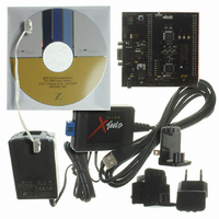
Z8 Encore! XP F1680 Series MCU for All Date Codes
The errata listed in
code. When reviewing the following errata, it is recommended that you download the most recent version
of the product specification, Z8 Encore! XP F1680 Series Product Specification (PS0250), from
www.zilog.com.
Table 1.Errata to the Z8 Encore! XP F1680 Series Devices
No. Summary
1
Voltage Brownout
Protection
Table 1
is found in the Z8 Encore! XP F1680 Series devices with any package date
Detailed Description
The VBO trip point specification for the Z8F1680 is 1.6 V to 1.8 V. Zilog does
not guarantee functionality of the product outside the operating range of 1.8 V
to 3.6 V. Because of this, there is a risk that the product might not function
properly before reaching the VBO threshold. Bits 5–7 of trim bit address
0003H are now “Reserved” to preserve the 1.6 V to 1.8 V VBO trip point spec-
ification.
Suggested Workarounds
1. Enable the “WDT Always On” Flash Option 0 bit 3 (VBO_AO) and the
“Flash Write Protect” Flash Option 0 bit 0 (FWP) features. If the device stops
functioning, then the WDT will automatically reset the device. The WDT nor-
mally requires the WDT instruction to start the WDT counting. If the device
happens to reset in a non-operational region, then the WDT instruction might
not get executed. Enabling the “WDT Always On” feature starts the WDT
counting upon application of system power. Enabling the “Flash Write Protect”
feature prevents the “WDT Always On”, the “Flash Write Protect” Flash option
bits, and the Flash Program Memory from getting erased or reprogrammed
accidentally when the device becomes nonfunctional. In summary, set
VBO_AO=0 and FWP=0.
2. If the user application requires erasing/programming of the Flash Program
Memory so that the “Flash Write Protect” feature cannot be used in the normal
operating supply voltage range, then the “Flash write operation protect” Flash
Option 1 bit 5 (FLASH_WR_PRO_EN) and the Low Voltage Detection (LVD)
feature can be used in conjunction with the Flash Option 0 “WDT Always On”
feature instead.
For example, the user selects the LVD threshold at 2.0 V. When the supply
voltage drops below 2.0 V and into a non-operational region, this triggers the
LVD to enable the “Flash Write Protect” Flash Option feature. The Flash Mem-
ory is now erase/program protected. If the device hangs up then the WDT will
continue to reset the device. The supply voltage now rises above the 2.0 V.
The LVD triggers the disable of the “Flash Write Protect” Flash Option feature.
The WDT timeout and device resets and continues proper execution.
Enabling these three features will protect the device, Flash Program Memory,
and Flash Option bits from corruption when the device is in a non-operational
supply voltage region. The LVD can be enabled in the Power Control Register
by setting bit 4 (LVD/VBO) option to 0. The “Flash write operation protect”
Flash Option 1 bit 5 (FLASH_WR_PRO_EN) is set to 1. In summary set LVD/
VBO=0, VBO_AO=0, and FLASH_WR_PRO_EN=1.
Copyright ©2010 by Zilog
UP008906-0810
www.zilog.com
Product Update
Errata for Z8 Encore! XP
Series Devices
®
, Inc. All rights reserved.
®
F1680


