NBSG11BAEVB ON Semiconductor, NBSG11BAEVB Datasheet - Page 2
NBSG11BAEVB
Manufacturer Part Number
NBSG11BAEVB
Description
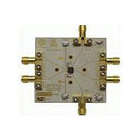
BOARD EVALUATION BBG NBSG11BA
Manufacturer
ON Semiconductor
Specifications of NBSG11BAEVB
Technology Type
Evaluation Board
Lead Free Status / RoHS Status
Contains lead / RoHS non-compliant
For Use With/related Products
NBSG11
Other names
NBSG11BAEVB
NBSG11BAEVBOS
NBSG11BAEVBOS


Table 1. PIN DESCRIPTION
*Devices in BGA package typically terminated with 50 W to V
1. The NC pins are electrically connected to the die and must be left open.
2. All V
3. In the differential configuration when the input termination pins (VTCLK, VTCLK) are connected to a common termination voltage, and
A2,A3,D2,
B2,C2
B3,C3
BGA
bottom (see case drawing) must be attached to a heat−sinking conduit.
if no signal is applied then the device will be susceptible to self−oscillation.
N/A
D1
C1
D3
C4
D4
B1
A1
A4
B4
D
C
CC
A
B
Figure 1. BGA−16 Pinout (Top View)
Pin
and V
VTCLK
VTCLK
CLK
CLK
6,7,14,15
EE
1
QFN
5,16
8,13
10
12
11
1
2
3
4
9
−
pins must be externally connected to Power Supply to guarantee proper operation. The thermally exposed pad on package
V
V
NC
NC
EE
EE
2
VTCLK
VTCLK
Name
CLK
CLK
V
V
NC
Q1
Q1
Q0
Q0
EP
CC
EE
V
V
NC
NC
CC
CC
3
LVCMOS, LVDS,
LVCMOS, LVDS,
RSECL Output
RSECL Output
RSECL Output
RSECL Output
LVTTL Input
LVTTL Input
Q1
Q1
Q0
Q0
ECL, CML,
ECL, CML,
4
I/O
−
−
−
−
−
−
http://onsemi.com
TT
Internal 50 W Termination Pin. See Table 2.
Inverted Differential Input. Internal 75 kW to V
Noninverted Differential Input. Internal 75 kW to V
Internal 50 W Termination Pin. See Table 2.
Negative Supply Voltage
No Connect
Positive Supply Voltage
Inverted Differential Output 1. Typically Terminated with 50 W to
V
Noninverted Differential Output 1. Typically Terminated with 50 W to
V
Inverted Differential output 0. Typically Terminated with 50 W to
V
Noninverted Differential Output 0. Typically Terminated with 50 W to
V
The Exposed Pad (EP) and the QFN−16 package bottom is thermally con-
nected to the die for improved heat transfer out of package. The exposed
pad must be attached to a heat−sinking conduit. The pad is not electrically
connected to the die but may be electrically and thermally connected to V
on the PC board.
TT
TT
TT
TT
= V
= V
= V
= V
= V
VTCLK
VTCLK
CC
2
CC
CC
CC
CC
CLK
CLK
− 1.5 V.
− 2.0 V*.
− 2.0 V*.
− 2.0 V*.
− 2.0 V*.
Figure 2. QFN−16 Pinout (Top View)
1
2
3
4
V
V
16
EE
5
EE
NC
15
NC
NBSG11
6
Description
NC
14
NC
7
V
V
13
8
CC
CC
EE
and 36.5 kW to V
EE
12
11
10
9
.
Q0
Q0
Q1
Q1
Exposed Pad (EP)
CC
.
EE
Related parts for NBSG11BAEVB
Image
Part Number
Description
Manufacturer
Datasheet
Request
R

Part Number:
Description:
Buffers & Line Drivers 2.5V/3.3V Multilevel
Manufacturer:
ON Semiconductor

Part Number:
Description:
ON Semiconductor [VOLTAGE REGULATOR]
Manufacturer:
ON Semiconductor
Datasheet:
Part Number:
Description:
357-036-542-201 CARDEDGE 36POS DL .156 BLK LOPRO
Manufacturer:
ON Semiconductor
Datasheet:
Part Number:
Description:
357-036-542-201 CARDEDGE 36POS DL .156 BLK LOPRO
Manufacturer:
ON Semiconductor
Datasheet:
Part Number:
Description:
357-036-542-201 CARDEDGE 36POS DL .156 BLK LOPRO
Manufacturer:
ON Semiconductor
Datasheet:
Part Number:
Description:
357-036-542-201 CARDEDGE 36POS DL .156 BLK LOPRO
Manufacturer:
ON Semiconductor
Datasheet:
Part Number:
Description:
357-036-542-201 CARDEDGE 36POS DL .156 BLK LOPRO
Manufacturer:
ON Semiconductor
Datasheet:
Part Number:
Description:
357-036-542-201 CARDEDGE 36POS DL .156 BLK LOPRO
Manufacturer:
ON Semiconductor
Datasheet:
Part Number:
Description:
357-036-542-201 CARDEDGE 36POS DL .156 BLK LOPRO
Manufacturer:
ON Semiconductor
Datasheet:
Part Number:
Description:
357-036-542-201 CARDEDGE 36POS DL .156 BLK LOPRO
Manufacturer:
ON Semiconductor
Datasheet:
Part Number:
Description:
357-036-542-201 CARDEDGE 36POS DL .156 BLK LOPRO
Manufacturer:
ON Semiconductor
Datasheet:
Part Number:
Description:
357-036-542-201 CARDEDGE 36POS DL .156 BLK LOPRO
Manufacturer:
ON Semiconductor
Datasheet:
Part Number:
Description:
Manufacturer:
ON Semiconductor
Datasheet: