NBSG14BAEVB ON Semiconductor, NBSG14BAEVB Datasheet
NBSG14BAEVB
Specifications of NBSG14BAEVB
NBSG14BAEVBOS


Related parts for NBSG14BAEVB


NBSG14BAEVB Summary of contents
Page 1
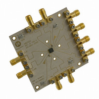
... Eye Pattern Generation Frequency Performance Output Rise and Fall Time V (Input High Common Mode Range) IHCMR 1. Single- ended measurements can only be made 3.3 V using this board setup Figure 1. NBSG14 Evaluation Board 1 http://onsemi.com EVALUATION BOARD MANUAL (1) or differential modes Publication Order Number: NBSG14BAEVB/D ...
Page 2
... EE -or -0.5 V (2.5 V op) EE All differential cable pairs must be matched. NOTE: Figure 2. NBSG14 Board Setup - Time Domain NBSG14BAEVB Setup for Time Domain Measurements Example Equipment (Note 1) HP6624A TDS8000 with 80E01 Sampling Head (Note 2) HP 8133A, Advantest D3186 Storm, Semflex CC Power Supply Connections 3 ...
Page 3
... OUT Amplitude = 500 Offset = 660 mV TRIGGER V = -1.3 V (3 -0.5 V (2.5 V op) EE NOTE: All differential cable pairs must be matched. Figure 3. NBSG14 Board Setup - Time Domain NBSG14BAEVB is within the V range. Refer to the device data sheet for further IH IHCMR ) to the Oscilloscope. The oscilloscope ...
Page 4
... NOTE: For frequency domain measurements, 2.5 V power supply is not recommended because additional equipment (bias tee, etc.) is needed for proper operation. The input signal has to be properly offset to meet V NBSG14BAEVB Example Equipment (Note 3) HP 6624A R&S ZVK (10 MHz to 40 GHz) Krytar Model #4010180 ...
Page 5
... Set input levels to -2.0 dBm (500 mV) at the input of DUT. Step 3: Output Setup 3a: Set display to measure S21 and record data. PORT 1 GND 50 W 1805 Hybrid Coupler V = -1.3 V (3.3 V op) EE Figure 4. NBSG14 Board Setup – Frequency Domain (Differential Mode) NBSG14BAEVB Rohde & Schwartz Vector Network Analyzer GND GND 2 ...
Page 6
... Set input levels to +2 dBm (500 mV) at the input of DUT. Output Setup Step 3: 3a: Set display to measure S21 and record data. PORT GND V = -1.3 V (3.3 V op) EE Figure 5. NBSG14 Board Setup – Frequency Domain (Single-Ended Mode) NBSG14BAEVB Rohde & Schwartz Vector Network Analyzer GND GND 2 ...
Page 7
... ROSENBERGER SMA T1 NOTE Decoupling cap (broadband cap with the range from 2 MHz to 30 GHz Transmission line NBSG14BAEVB The following considerations played a key role to ensure this evaluation board achieves high-end microwave performance: Optimal SMA connector launch Minimal insertion loss and signal dispersion ...
Page 8
... Dielectric (5.0 mil) Thick Copper Base Figure 7. Board Stack- START 1 GHz NOTE: The insertion loss curve can be used to calibrate out board loss if testing under small signal conditions. NBSG14BAEVB Manufacturer ON Semiconductor Rosenberger Dielectric Laboratories 32 mil PIN 1 Figure 8. Layout Mask for NBSG14 1 GHz/ Figure 9 ...
Page 9
... FREQUENCY (GHz) Figure 10. Fmax - Amplitude vs. Frequency (NBSG14 3 255C -40 Figure 12. NBSG14 T Figure 13. NBSG14: Eye Diagram at 10 Gbps with PRBS 2^31-1 (total Pk-Pk system jitter including signal generator is 18 ps) NBSG14BAEVB -40 -20 Figure 11. NBSG14 T 3.3 V 2 TEMPERATURE ( C) vs. Temperature and Supply Voltage f http://onsemi.com 9 – ...
Page 10
... START 10 MHz 1 GHz/ Figure 14. NBSG14: Small Signal Gain (S21) Q0-Q1B 10 dB -40 dB START 10 MHz 1 GHz/ Figure 16. NBSG14 Return Loss (S11) Q0 – Q1B NBSG14BAEVB CC 11 GHz 25 dB -25 dB STOP 12 GHz START 1 GHz Figure 15. NBSG14: Large Signal Gain (S21) 11 GHz 10 dB -40 dB ...
Page 11
... SiGe Differential 1:4 Clock/Data Driver with RSECL Outputs NBSG14BA 2.5V/3.3V SiGe Differential 1:4 Clock/Data Driver with RSECL Outputs NBSG14BAEVB NBSG14 Evaluation Board NBSG14BAEVB References NBSG14/D, Data Sheet, NBSG14, 2.5V/3.3V SiGe 1:4 Differential Clock Driver with RSECL Outputs AND8077/D, Application Note, GigaCommt (SiGe) SPICE Modeling Kit. AND8075/D, Application Considerations for the FCBGA Packages ...
Page 12
... DATUM Z (SEATING PLANE) IS DEFINED BY THE SPHERICAL CROWNS OF THE SOLDER BALLS. 5. PARALLELISM MEASUREMENT SHALL EXCLUDE ANY EFFECT OF MARK ON TOP SURFACE OF PACKAGE. MILLIMETERS DIM MIN MAX A 1.40 MAX A1 0.25 0.35 A2 1.20 REF b 0.30 0.50 D 4.00 BSC E 4.00 BSC e 1.00 BSC S 0.50 BSC NBSG14BAEVB/D ...