NBSG72AMNEVB ON Semiconductor, NBSG72AMNEVB Datasheet - Page 3
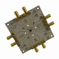
NBSG72AMNEVB
Manufacturer Part Number
NBSG72AMNEVB
Description
BOARD EVAL BBG NBSG72AMN
Manufacturer
ON Semiconductor
Specifications of NBSG72AMNEVB
Lead Free Status / RoHS Status
Contains lead / RoHS non-compliant
For Use With/related Products
NBSG72AMN/D
Other names
NBSG72AMNEVB
NBSG72AMNEVBOS
NBSG72AMNEVBOS


3. When an output level of 400 mV is desired and V
Table 3. OUTPUT LEVEL SELECT (OLS)
Table 4. INTERFACING OPTIONS
VTD0
D0
D0
D1
D1
VTD1
SELA
SELB
OLS
50 W
50 W
RSECL, PECL, NECL
Interfacing Options
LVCMOS / LVTTL
AC−COUPLED
V
75 kW
V
V
V
75 kW
EE
CC
CC
CC
50 W
50 W
FLOAT
LVDS
OLS
CML
V
(Note 3)
− 0.4 V
− 0.8 V
− 1.2 V
CC
Figure 2. Logic/Block Diagram
2
2
2
2
2
2
2
2
Connect VTD0 and VTD1 to V
VTD0 and VTD1 Should Be Left Floating.
Bias VTD0 and VTD1 Inputs within Common Mode Range (VIHCMR)
Standard ECL Termination Techniques
The external voltage should be applied to the unused complementary differential input.
Nominal voltage is 1.5 V for LVTTL and V
2
2
CC
Output Amplitude (V
− V
http://onsemi.com
EE
> 3.0 V, a 2 kW resistor should be connected from OLS to V
800 mV
200 mV
600 mV
400 mV
600 mV
V
V
3
0
CC
EE
CC
Q0
Q0
Q1
Q1
OUTPP
+
)
Connections
CC
/2 for LVCMOS Inputs.
Table 2. TRUTH TABLE
SELA
HIGH
HIGH
LOW
LOW
SELB
HIGH
HIGH
LOW
LOW
OLS Sensitivity
OLS ± 150 mV
OLS ± 100 mV
OLS ± 100 mV
OLS − 75 mV
OLS ± 75 mV
N/A
Q0
D1
D0
D1
D0
EE
.
Q1
D0
D0
D1
D1
Related parts for NBSG72AMNEVB
Image
Part Number
Description
Manufacturer
Datasheet
Request
R

Part Number:
Description:
ON Semiconductor [VOLTAGE REGULATOR]
Manufacturer:
ON Semiconductor
Datasheet:
Part Number:
Description:
357-036-542-201 CARDEDGE 36POS DL .156 BLK LOPRO
Manufacturer:
ON Semiconductor
Datasheet:
Part Number:
Description:
357-036-542-201 CARDEDGE 36POS DL .156 BLK LOPRO
Manufacturer:
ON Semiconductor
Datasheet:
Part Number:
Description:
357-036-542-201 CARDEDGE 36POS DL .156 BLK LOPRO
Manufacturer:
ON Semiconductor
Datasheet:
Part Number:
Description:
357-036-542-201 CARDEDGE 36POS DL .156 BLK LOPRO
Manufacturer:
ON Semiconductor
Datasheet:
Part Number:
Description:
357-036-542-201 CARDEDGE 36POS DL .156 BLK LOPRO
Manufacturer:
ON Semiconductor
Datasheet:
Part Number:
Description:
357-036-542-201 CARDEDGE 36POS DL .156 BLK LOPRO
Manufacturer:
ON Semiconductor
Datasheet:
Part Number:
Description:
357-036-542-201 CARDEDGE 36POS DL .156 BLK LOPRO
Manufacturer:
ON Semiconductor
Datasheet:
Part Number:
Description:
357-036-542-201 CARDEDGE 36POS DL .156 BLK LOPRO
Manufacturer:
ON Semiconductor
Datasheet:
Part Number:
Description:
357-036-542-201 CARDEDGE 36POS DL .156 BLK LOPRO
Manufacturer:
ON Semiconductor
Datasheet:
Part Number:
Description:
357-036-542-201 CARDEDGE 36POS DL .156 BLK LOPRO
Manufacturer:
ON Semiconductor
Datasheet:
Part Number:
Description:
Manufacturer:
ON Semiconductor
Datasheet:
Part Number:
Description:
Manufacturer:
ON Semiconductor
Datasheet:
Part Number:
Description:
Manufacturer:
ON Semiconductor
Datasheet: