TC642EV Microchip Technology, TC642EV Datasheet - Page 10
TC642EV
Manufacturer Part Number
TC642EV
Description
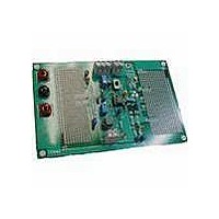
KIT EVALUATION FOR TC642
Manufacturer
Microchip Technology
Specifications of TC642EV
Processor To Be Evaluated
TC642 and TC646
Lead Free Status / RoHS Status
Lead free / RoHS Compliant
Lead Free Status / RoHS Status
Lead free / RoHS Compliant, Lead free / RoHS Compliant
Other names
Q698359


TC642
FIGURE 5-2:
Circuit.
Generally, the thermistor shown in Figure 5-2 is a non-
linear device with a negative temperature coefficient
(also called an NTC thermistor). In Figure 5-2, R
used to linearize the thermistor temperature response,
while R
coefficient at the V
configuration produces an output voltage delta of 1.4V,
which is well within the range of the V
specification of the TC642. A 100 k NTC thermistor is
selected for this application in order to keep I
minimum.
For the voltage range at V
2.65V, the temperature range of this configuration is
0°C to 50°C. If a different temperature range is required
from this circuit, R
resistance value of the thermistor at the center of this
new temperature range. With this change, R
adjusted according to the formulas below. It is
suggested that a maximum temperature range of 50°C
be used with this circuit due to thermistor linearity
limitations.
The following two equations permit solving for the two
unknown variables, R
regarding thermistors can be found in AN679, “Temper-
ature Sensing Technologies”, and AN685, “Thermistors
in Single Supply Temperature Sensing Circuits”, which
can be downloaded from Microchip’s web site at:
www.microchip.com.
EQUATION
DS21444C-page 10
Where T
R
and R
TEMP
NTC Thermistor
100 k @ 25˚C
1
2
.
is the parallel combination of the thermistor
is used to produce a positive temperature
1
and T
R
RT
R
TEMP
TEMP
1
V
V
2
DD
DD
IN
1
are the chosen temperatures and
(T
(T
should be chosen to equal the
node. As an added benefit, this
x R
x R
Temperature Sensing
2
1
1
) + R
) + R
2
2
and R
IN
2
2
V
to be equal to 1.25V to
DD
= V(T
= V(T
2
R
R
. More information
I
DIV
1
2
= 100 k
= 23.2 k
2
1
)
)
V
DIV
C(SPAN)
IN
2
at a
1
is
is
5.2
A voltage divider on V
cycle and, thus, the minimum fan speed. As with the
V
to 100% duty cycle. Assuming that fan speed is linearly
related to duty cycle, the minimum speed voltage is
given by the equation:
EQUATION
For example, if 2500 RPM equates to 100% fan speed,
and a minimum speed of 1000 RPM is desired, then
the V
EQUATION
The V
divider, as shown in Figure 5-3. Per Section 1.0,
“Electrical Characteristics”, the leakage current at the
V
conservative to design for a divider current, I
100 µA. If V
EQUATION
FIGURE 5-3:
IN
MIN
input, 1.25V to 2.65V typically corresponds to 0%
MIN
pin is no more than 1 µA. It would be very
MIN
V
V
MIN
I
MIN
DIV
Minimum Fan Speed
voltage is:
voltage may be set using a simple resistor
R
=
DD
=
1
= 100µA =
+ R
= 5.0V then;
Minimum Speed
I
DIV
2500
1000
2
Full Speed
=
GND
V
DD
MIN
V
100µA
5.0V
R
IN
R
R
2
sets the minimum PWM duty
1
x (1.4) + 1.25V = 1.81V
1
2002 Microchip Technology Inc.
+ R
5.0V
Circuit.
V
MIN
= 50,000 = 50k
2
I
IN
, therefore
x (1.4) + 1.25V
DIV
, of
Related parts for TC642EV
Image
Part Number
Description
Manufacturer
Datasheet
Request
R

Part Number:
Description:
DEMO BOARD FOR TC642/46/47/48/49
Manufacturer:
Microchip Technology
Datasheet:

Part Number:
Description:
Manufacturer:
Microchip Technology Inc.
Datasheet:
Part Number:
Description:
Manufacturer:
Microchip Technology Inc.
Datasheet:
Part Number:
Description:
Manufacturer:
Microchip Technology Inc.
Datasheet:
Part Number:
Description:
Manufacturer:
Microchip Technology Inc.
Datasheet:
Part Number:
Description:
Manufacturer:
Microchip Technology Inc.
Datasheet:
Part Number:
Description:
Manufacturer:
Microchip Technology Inc.
Datasheet:
Part Number:
Description:
Manufacturer:
Microchip Technology Inc.
Datasheet:
Part Number:
Description:
Manufacturer:
Microchip Technology Inc.
Datasheet: