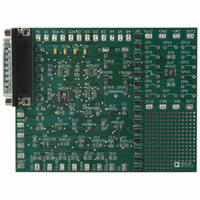
AD5263EVAL Analog Devices Inc, AD5263EVAL Datasheet - Page 6

AD5263EVAL
Manufacturer Part Number
AD5263EVAL
Description
BOARD EVAL FOR AD5263
Manufacturer
Analog Devices Inc
Datasheet
1.AD5263BRUZ200.pdf
(28 pages)
Specifications of AD5263EVAL
Rohs Status
RoHS non-compliant
Main Purpose
Digital Potentiometer
Embedded
No
Utilized Ic / Part
AD5263
Primary Attributes
4 Channel, 256 Position
Secondary Attributes
I²C & SPI Interfaces
Lead Free Status / Rohs Status
Not Compliant
AD5263
ABSOLUTE MAXIMUM RATINGS
T
Table 3.
Parameter
V
V
V
V
V
Terminal Current, Ax to Bx, Ax to Wx, Bx to Wx
Digital Inputs and Output Voltage to GND
Operating Temperature Range
Maximum Junction Temperature (T
Storage Temperature Range
Reflow Soldering
Thermal Resistance
1
2
Maximum terminal current is bounded by the maximum current handling of
Package power dissipation: (T
the switches, maximum power dissipation of the package, and maximum
applied voltage across any two of the A, B, and W terminals at a given
resistance.
DD
SS
DD
L
A
A
, V
to GND
Pulsed
Continuous
Peak Temperature
Time at Peak Temperature
TSSOP-24
to GND
= 25°C, unless otherwise noted.
to GND
to V
B
, V
W
SS
1
to GND
2
θ
JA
JMAX
− T
A
)/θ
JA
JMAX
.
)
Value
−0.3 V to +16.5 V
−7.5 V to 0 V
+16.5 V
−0.3 V to +6.5 V
V
±20 mA
±3 mA
0 V to +7 V
−40°C to +85°C
150°C
−65°C to +150°C
260°C
20 sec to 40 sec
143°C/W
SS
to V
DD
Rev. B | Page 6 of 28
Stresses above those listed under Absolute Maximum Ratings
may cause permanent damage to the device. This is a stress
rating only; functional operation of the device at these or any
other conditions above those indicated in the operational
section of this specification is not implied. Exposure to absolute
maximum rating conditions for extended periods may affect
device reliability.
ESD CAUTION


