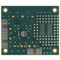
AD629-EVAL Analog Devices Inc, AD629-EVAL Datasheet - Page 11

AD629-EVAL
Manufacturer Part Number
AD629-EVAL
Description
BOARD EVAL COMMON MODE AD629
Manufacturer
Analog Devices Inc
Type
Amplifiers: OP Ampsr
Datasheet
1.AD629-EVAL.pdf
(16 pages)
Specifications of AD629-EVAL
Design Resources
Measuring -48 V High-Side Current Using AD629, AD8603, AD780, and AD7453 (CN0100)
Contents
Evaluation Board
For Use With/related Products
AD629
Lead Free Status / RoHS Status
Contains lead / RoHS non-compliant
+IN
–IN
+IN
–IN
If there is only a single power supply available, it must be shared
by both digital and analog circuitry. Figure 33 shows how to
minimize interference between the digital and analog circuitry.
In this example, the ADC’s reference is used to drive Pin REF(+)
and Pin REF(–). This means that the reference must be capable
of sourcing and sinking a current equal to V
the previous case, separate analog and digital ground planes
should be used (reasonably thick traces can be used as an
alternative to a digital ground plane). These ground planes
should connect at the power supply’s ground pin. Separate
traces (or power planes) should run from the power supply to
the supply pins of the digital and analog circuits. Ideally, each
device should have its own power supply trace, but these can be
shared by a number of devices, as long as a single trace is not
used to route current to both digital and analog circuitry.
USING A LARGE SENSE RESISTOR
Insertion of a large value shunt resistance across the input pins,
Pin 2 and Pin 3, will imbalance the input resistor network,
introducing a common-mode error. The magnitude of the error
will depend on the common-mode voltage and the magnitude
of R
Table 4. Recommended Values for 2-Pole Butterworth Filter
Corner Frequency
No Filter
50 kHz
5 kHz
500 Hz
50 Hz
Figure 32. Optimal Grounding Practice for a Bipolar Supply Environment
Figure 33. Optimal Ground Practice in a Single-Supply Environment
SHUNT
3
2
3
2
AD629
AD629
4
REF(–) REF(+)
REF(–) REF(+)
–V
+V
0.1µF
.
1
7
S
1
S
0.1µF
OUTPUT
OUTPUT
0.1µF
with Separate Analog and Digital Supplies
–V
+V
4
5
5
–5V
S
S
ANALOG POWER
7
6
6
SUPPLY
R1
2.94 kΩ ± 1%
2.94 kΩ ± 1%
2.94 kΩ ± 1%
2.7 kΩ ± 10%
+5V
POWER SUPPLY
V
V
4
3
V
+5V
IN1
IN2
DD
V
V
V
0.1µF
IN1
IN2
DD
1
GND
0.1µF
AGND DGND
AGND
GND
AD7892-2
ADC
6
DGND
14
CM
12
/200 kΩ. As in
R2
1.58 kΩ ± 1%
1.58 kΩ ± 1%
1.58 kΩ ± 1%
1.5 kΩ ± 10%
MICROPROCESSOR
MICROPROCESSOR
POWER SUPPLY
V
DD
GND
GND
0.1µF
DIGITAL
0.1µF
GND
+5V
V
DD
Rev. B | Page 11 of 16
C1
2.2 nF ± 10%
22 nF ± 10%
220 nF ± 10%
2.2 μF ± 20%
Table 3 shows some sample error voltages generated by a
common-mode voltage of 200 V dc with shunt resistors from
20 Ω to 2000 Ω. Assuming that the shunt resistor is selected to
use the full ±10 V output swing of the AD629, the error voltage
becomes quite significant as R
Table 3. Error Resulting from Large Values of R
(Uncompensated Circuit)
R
20
1000
2000
To measure low current or current near zero in a high common-
mode environment, an external resistor equal to the shunt
resistor value can be added to the low impedance side of the
shunt resistor, as shown in Figure 34.
OUTPUT FILTERING
A simple 2-pole, low-pass Butterworth filter can be implemented
using the OP177 after the AD629 to limit noise at the output, as
shown in Figure 35. Table 4 gives recommended component
values for various corner frequencies, along with the peak-to-
peak output noise for each case.
–V
0.1µF
S
S
+IN
(Ω)
–IN
REF (–)
Figure 35. Filtering of Output Noise Using a 2-Pole Butterworth Filter
I
SHUNT
1
2
3
4
NC = NO CONNECT
Figure 34. Compensating for Large Sense Resistors
21.1kΩ
380kΩ
380kΩ
Error V
0.01
0.498
1
–V
S
R
R
C2
1 nF ± 10%
10 nF ± 10%
0.1 μF ± 10%
1 μF ± 20%
COMP
SHUNT
AD629
380kΩ
20kΩ
OUT
0.1µF
REF (–)
(V)
–V
+IN
–IN
8
7
6
5
S
NC
+V
REF (+)
1
2
3
4
S
NC = NO CONNECT
+V
21.1kΩ
380kΩ
380kΩ
SHUNT
R1
0.1µF
S
increases.
Error Indicated (mA)
0.5
0.498
0.5
AD629
380kΩ
20kΩ
Output Noise (p-p)
3.2 mV
1 mV
0.32 mV
100 μV
32 μV
C1
R2
C2
8
7
6
5
OP177
NC
+V
REF (+)
+V
–V
S
S
S
V
SHUNT
+V
OUT
0.1µF
0.1µF
S
0.1µF
AD629
V
OUT


