AD8330-EVAL Analog Devices Inc, AD8330-EVAL Datasheet
AD8330-EVAL
Specifications of AD8330-EVAL


Related parts for AD8330-EVAL


AD8330-EVAL Summary of contents
Page 1
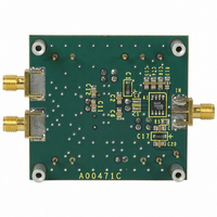
... Figure 2). For convenience, the board includes an AD8131 ended signal source to the differential input of the AD8330. If desired, the AD8131 can be removed and the AD8330 can be driven at one of its inputs from a single-ended source. The AD8330 output is observed at the SMA connectors OUT_HI and OUT_LO or by using the 2-pin header OUT_HI/ OUT_LO adjacent to the device ...
Page 2
... OUT_HI and OUT_LO can also be used, but the user may need to account for load capacitance effects. EVAL-AD8330EB BOARD DESIGN The EVAL-AD8330EB is a 4-layer design for maximum ground- plane area. The evaluation board side silkscreen and wiring patterns are shown in Figure 4 through Figure 9. ...
Page 3
... Figure 4. Component-Side Silkscreen Figure 5. Component-Side Wiring Figure 6. Inner Layer 1 Figure 7. Wiring-Side Silkscreen Figure 8. Wiring-Side Pattern Figure 9. Inner Layer 2 Rev Page EVAL-AD8330EB ...
Page 4
... ESD protection circuitry, permanent damage may occur on devices subjected to high energy electrostatic discharges. Therefore, proper ESD precautions are recommended to avoid performance degradation or loss of functionality. ORDERING GUIDE Model AD8330-EVAL ©2006 Analog Devices, Inc. All rights reserved. Trademarks and registered trademarks are the property of their respective owners. Reference Designator R5 ...