AD8369-EVAL Analog Devices Inc, AD8369-EVAL Datasheet - Page 13
AD8369-EVAL
Manufacturer Part Number
AD8369-EVAL
Description
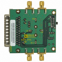
BOARD EVAL FOR AD8369
Manufacturer
Analog Devices Inc
Datasheet
1.AD8369-EVAL.pdf
(24 pages)
Specifications of AD8369-EVAL
Lead Free Status / RoHS Status
Contains lead / RoHS non-compliant


THEORY OF OPERATION
The AD8369 is a digitally controlled fully differential VGA
based on a variation of Analog Devices’ patented X-AMP archi-
tecture (Figure 1). It provides accurate gain control over a 45 dB
span with a constant –3 dB bandwidth of 600 MHz.
The 3 dB gain steps can be controlled by a user-selectable
parallel- or serial-mode digital interface. A single pin (SENB)
selects the mode. The AD8369 is designed for optimal
operation when used in a fully differential system, although
single-ended operation is also possible. Its nominal input and
output impedances are 200 W.
Input Attenuator and Output 3 dB Step
The AD8369 is comprised of a seven-stage R-2R ladder net-
work (eight taps) and a selected Gm stage followed by a
fixed-gain differential amplifier. The ladder provides a total
attenuation of 42 dB in 6 dB steps. The full signal is applied to
the amplifier using the first tap; at the second tap, the signal
is 6 dB lower and so on. A further 3 dB interpolating gain step is
introduced at the output of the fixed gain amplifier, providing
the full 45 dB of gain span.
Fixed Gain Amplifier
The fixed gain amplifier is driven by the tap point of the R-2R
ladder network via the selected Gm cell. The output stage is a
REV. 0
CMDC
DIGITAL
INLO
INHI
Figure 1. General Block Diagram, Control and Signal Paths Are Differential
GAIN STEP SELECTION
Gm CELLS
TPC 37. Power Supply Rejection Ratio, V
R
100
L
90
80
70
60
50
40
30
20
10
0
= 1 k W , Maximum Gain
10
100
FREQUENCY – kHz
–13–
~
V
FIXED
2
GAIN
S
– 0.7
complementary pair of current sources, loaded with internal
100 W resistors to ac ground which provides a 200 W differential
output impedance. The low frequency gain of the AD8369
can be approximated by the equation:
where R
code; 0 is the minimum gain code and 15 is the maximum gain
code. The external load, which is in parallel combination with
the internal 200 W output resistor, affects the overall gain and
peak output swing. Note that the external load has no effect on the
gain step size.
Input and Output Interfaces
The dc working points of the differential input and output inter-
faces of the AD8369 are internally biased. The inputs INHI and
INLO are biased to a diode drop below V
positive supply) to meet isolation and headroom constraints,
while the outputs OPHI and OPLO are centered on the supply
midpoint, V
The internal V
ered and decoupled to ground via internal capacitors. The
input bias voltage, derived from this V
20pF
1000
L
is the external load resistor in ohms and n is the gain
3dB SWITCHED
ATTENUATOR
S
/2, to provide the maximum output swing.
V
V
BIAS
S
OUT
/2 reference and the CMDC reference are buff-
IN
S
= 5 V,
10000
=
0 6
.
Ê
Á
Ë
V
200
S
200
/2
+
R
R
L
V
V
L
S
S
ˆ
˜
¯
100
100
Ê
Á
Á
Ë
S
/2 reference, is brought
S
2
/2 (~1.7 V for a 5 V
(
15
1
V
-
S
22pF
n
AD8369
/2
)
OPHI
OPLO
ˆ
˜
˜
¯
Related parts for AD8369-EVAL
Image
Part Number
Description
Manufacturer
Datasheet
Request
R

Part Number:
Description:
BOARD EVAL FOR AD8369 LF-600MHZ
Manufacturer:
Analog Devices Inc

Part Number:
Description:
±1.7g Dual-Axis IMEMS Accelerometer Evaluation Board
Manufacturer:
Analog Devices Inc
Datasheet:
Part Number:
Description:
Inertial Sensor Evaluation System
Manufacturer:
Analog Devices Inc
Datasheet:
Part Number:
Description:
Manufacturer:
Analog Devices Inc
Datasheet:
Part Number:
Description:
Manufacturer:
Analog Devices Inc
Datasheet:
Part Number:
Description:
Manufacturer:
Analog Devices Inc
Datasheet:
Part Number:
Description:
Manufacturer:
Analog Devices Inc
Datasheet:
Part Number:
Description:
Manufacturer:
Analog Devices Inc
Datasheet:
Part Number:
Description:
Manufacturer:
Analog Devices Inc
Datasheet:
Part Number:
Description:
Manufacturer:
Analog Devices Inc
Datasheet:
Part Number:
Description:
Manufacturer:
Analog Devices Inc
Datasheet:
Part Number:
Description:
Manufacturer:
Analog Devices Inc
Datasheet:
Part Number:
Description:
Manufacturer:
Analog Devices Inc
Datasheet: