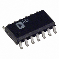
ADXL250EB Analog Devices Inc, ADXL250EB Datasheet - Page 2

ADXL250EB
Manufacturer Part Number
ADXL250EB
Description
IC ACCELER DUAL-AX 50G 8-CLCC
Manufacturer
Analog Devices Inc
Series
iMEMS®r
Specifications of ADXL250EB
Rohs Status
RoHS non-compliant
Axis
X, Y
Acceleration Range
±50g
Sensitivity
38mV/g
Voltage - Supply
*
Output Type
Analog
Bandwidth
1kHz
Mounting Type
Surface Mount
Lead Free Status / RoHS Status
Not Compliant
ADXL150/ADXL250–SPECIFICATIONS
Parameter
SENSOR
SENSITIVITY
ZERO g BIAS LEVEL
ZERO-g OFFSET ADJUSTMENT
NOISE PERFORMANCE
FREQUENCY RESPONSE
SELF-TEST
OUTPUT AMPLIFIER
POWER SUPPLY (V
TEMPERATURE RANGE
NOTES
1
2
3
4
5
6
7
Specifications subject to change without notice.
Alignment error is specified as the angle between the true axis of sensitivity and the edge of the package.
Transverse sensitivity is measured with an applied acceleration that is 90 degrees from the indicated axis of sensitivity.
Ratiometric: V
Ratiometric, proportional to V
See Figure 11 and Device Bandwidth vs. Resolution section.
Self-test output varies with supply voltage.
When using ADXL250, both Pins 13 and 14 must be connected to the supply for the device to function.
doubled by connecting V
Guaranteed Full-Scale Range
Nonlinearity
Package Alignment Error
Sensor-to-Sensor Alignment Error
Transverse Sensitivity
Sensitivity (Ratiometric)
Sensitivity Drift Due to Temperature Delta from 25 C to T
Output Bias Voltage
Zero g Drift Due to Temperature
Voltage Gain
Input Impedance
Noise Density
Clock Noise
–3 dB Bandwidth
Bandwidth Temperature Drift
Sensor Resonant Frequency
Output Change
Logic “1” Voltage
Logic “0” Voltage
Input Resistance
Output Voltage Swing
Capacitive Load Drive
Functional Voltage Range
Quiescent Supply Current
Operating Range J
Specified Performance A
OUT
5
= V
6
S
/2 + (Sensitivity
S
4
)
OUT
7
2
3
to the offset null pin.
1
S
/2. See Figure 21.
V
Conditions
Y Channel
X Channel
Delta from 25 C to T
Delta V
T
Q = 5
ST Pin from Logic “0” to “1”
To Common
I
ADXL150
ADXL250 (Total 2 Channels)
S
OUT
/5 V
MIN
= 100 A
to T
a) where a = applied acceleration in gs, and V
OUT
MAX
/Delta V
OS PIN
MIN
MIN
or T
or T
MAX
MAX
–2–
Min
33.0
V
0.45
20
900
0.25
V
30
0.25
1000
4.0
0
–40
40
S
S
/2 – 0.35 V
ADXL150JQC/AQC
– 1
(T
V
S
A
= +5.00 V, Acceleration = Zero g , unless otherwise noted)
= +25 C for J Grade, T
S
= supply voltage. See Figure 21. Output scale factor can be
Typ
0.2
38.0 43.0
0.2
0.50 0.55
30
1
5
1000
50
24
0.40 0.60
50
1.8
50
1
2
0.5
S
/2
Max
V
2.5
1.0
V
6.0
3.0
+70
+85
S
S
/2 + 0.35 V
– 0.25
A
Min
33.0
33.0
0.45
20
900
0.25
V
30
0.25
1000
4.0
0
–40
= –40 C to +85 C for A Grade,
40
S
S
ADXL250JQC/AQC
/2 – 0.35 V
– 1
Typ Max
0.2
38.0 43.0
38.0 43.0
0.3
0.50 0.55
30
1
5
1000
50
24
0.40 0.60
50
3.5
50
1
0.1
2
0.5
S
/2 V
2.5
1.0
V
6.0
5.0
+70
+85
S
S
/2 + 0.35 V
– 0.25
REV. 0
Units
g
% of FS
Degrees
Degrees
%
mV/g
mV/g
%
g
V/V
k
mg/ Hz
mV p-p
Hz
Hz
kHz
V
V
V
k
V
pF
V
mA
mA
C
C


