EVAL-AD7864-1CB Analog Devices Inc, EVAL-AD7864-1CB Datasheet - Page 8
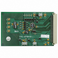
EVAL-AD7864-1CB
Manufacturer Part Number
EVAL-AD7864-1CB
Description
BOARD EVAL FOR AD7864-1
Manufacturer
Analog Devices Inc
Datasheet
1.AD7864ASZ-1.pdf
(28 pages)
Specifications of EVAL-AD7864-1CB
Number Of Adc's
1
Number Of Bits
12
Sampling Rate (per Second)
520k
Data Interface
Parallel
Inputs Per Adc
4 Differential
Input Range
±10 V
Power (typ) @ Conditions
90mW @ 520kSPS
Voltage Supply Source
Analog and Digital
Operating Temperature
-40°C ~ 85°C
Utilized Ic / Part
AD7864-1
Lead Free Status / RoHS Status
Contains lead / RoHS non-compliant


AD7864
Pin No.
27
28
29 to 34
35
36
37
38, 39
40 to 43
44
Mnemonic
INT /EXT CLK
CLKIN
DB11 to DB6
DV
V
DGND
DB5, DB4
DB3 to DB0
EOC
DRIVE
DD
Description
Internal/External Clock Select Input. When this pin is at Logic 0, the AD7864 uses its internally generated master
clock. When this pin is at Logic 1, the master clock is generated externally to the device.
Conversion Clock Input. This is an externally applied clock that allows the user to control the conversion rate of
the AD7864. Each conversion needs 14 clock cycles for the conversion to be completed and an EOC pulse to be
generated. The clock should have a duty cycle that is no worse than 60/40. See the
section.
Data Bit 11 is the MSB, followed by Data Bit 10 to Data Bit 6. Three-state TTL outputs. Output coding is twos
complement for the AD7864-1 and AD7864-3. Output coding is straight (natural) binary for the AD7864-2.
Positive Supply Voltage for Digital Section, 5.0 V ± 5%. Connect a 0.1 μF decoupling capacitor between this pin
and AGND. Both DV
This pin provides the positive supply voltage for the output drivers (DB0 to DB11), BUSY, EOC , and FRSTDATA. It
is normally tied to DV
the conversion sequence. To facilitate interfacing to 3 V processors and DSPs, the output data drivers can also be
powered by a 3 V ± 10% supply.
Digital Ground. This is the ground reference for digital circuitry. Connect this DGND pin to the AGND plane of
the system at the AGND pin.
Data Bit 5 to Data Bit 4. Three-state TTL outputs.
Data Bit 3 to Data Bit 0. Bidirectional data pins. When a read operation takes place, these pins are three-state TTL
outputs. The channel select register is programmed with the data on the DB0 to DB3 pins with standard CS and
WR signals. DB0 represents Channel 1, and DB3 represents Channel 4.
End-of-Conversion. Active low logic output indicating conversion status. The end of each conversion in a
conversion sequence is indicated by a low-going pulse on this line.
DD
DD
and AV
. Decouple V
DD
should be externally tied together.
Rev. D | Page 8 of 28
DRIVE
with a 0.1 μF capacitor to improve performance when reading during
Using An External Clock
Related parts for EVAL-AD7864-1CB
Image
Part Number
Description
Manufacturer
Datasheet
Request
R


Part Number:
Description:
BOARD EVAL FOR SI270X-A
Manufacturer:
Silicon Laboratories Inc
Datasheet:

Part Number:
Description:
BUCK CONV REF DESIGN KIT IP1201
Manufacturer:
International Rectifier
Datasheet:
Part Number:
Description:
BOARD DEMO SYNC DUAL BUCK CNVTER
Manufacturer:
International Rectifier
Datasheet:
Part Number:
Description:
BOARD DEMO SYNC BUCK CONVETER
Manufacturer:
International Rectifier
Datasheet:

Part Number:
Description:
EVALBOARD/EB Omnidirectional microphone - Analog
Manufacturer:
Analog Devices
Datasheet:
Part Number:
Description:
EVALBOARD/EB Omnidirectional microphone - Analog
Manufacturer:
Analog Devices
Datasheet:


Part Number:
Description:
BOARD EVAL LED DRIVER LT3756
Manufacturer:
Linear Technology
Datasheet:

Part Number:
Description:
BOARD EVAL FOR AD7741/7742
Manufacturer:
Analog Devices Inc
Datasheet:

Part Number:
Description:
±1.7g Dual-Axis IMEMS Accelerometer Evaluation Board
Manufacturer:
Analog Devices Inc
Datasheet:

Part Number:
Description:
IC MULTIPLIER ANALOG 8-SOIC T/R
Manufacturer:
Analog Devices Inc
Datasheet:

Part Number:
Description:
IC ANALOG MULTIPLIER 8-DIP
Manufacturer:
Analog Devices Inc
Datasheet:
Part Number:
Description:
IC ANALOG MULTIPLIER 8-SOIC
Manufacturer:
Analog Devices Inc
Datasheet:
Part Number:
Description:
IC ANALOG MULTIPLIER 8-DIP
Manufacturer:
Analog Devices Inc
Datasheet: