AD9956/PCB Analog Devices Inc, AD9956/PCB Datasheet - Page 2
AD9956/PCB
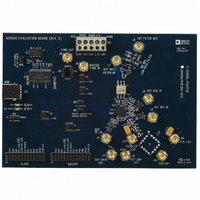
Manufacturer Part Number
AD9956/PCB
Description
BOARD EVAL FOR AD9956
Manufacturer
Analog Devices Inc
Datasheet
1.AD9956YCPZ.pdf
(32 pages)
Specifications of AD9956/PCB
Module/board Type
Evaluation Board
For Use With/related Products
AD9956
Lead Free Status / RoHS Status
Contains lead / RoHS non-compliant


AD9956
TABLE OF CONTENTS
Product Overview............................................................................. 3
Specifications..................................................................................... 4
Absolute Maximum Ratings.......................................................... 10
Pin Configuration and Function Descriptions........................... 11
Typical Performance Characteristics ........................................... 13
Typical Application Circuits.......................................................... 16
General Description ....................................................................... 18
REVISION HISTORY
9/04—Data Sheet Changed from Rev. 0 to Rev. A
Changes to the Pin Configuration................................................ 11
Changes to the Pin Function Descriptions ................................. 12
Changes to Table 5.......................................................................... 24
Changes to CFR2<15:12> PLLREF Divider
Control Bits (÷N)............................................................................ 31
Changes to CFR2<11:8> PLLREF Divider
Control Bits (÷M)........................................................................... 31
Changes to Ordering Guide .......................................................... 32
7/04—Revision: Initial Version
Loop Measurement Conditions.................................................. 9
ESD Caution................................................................................ 10
Application Circuit Explanations............................................. 17
DDS Core..................................................................................... 18
PLL Circuitry .............................................................................. 18
Rev. A | Page 2 of 32
Modes of Operation ....................................................................... 20
Serial Port Operation ..................................................................... 22
Register Map and Description ...................................................... 24
Outline Dimensions ....................................................................... 32
CML Driver................................................................................. 19
DDS Modes of Operation ......................................................... 20
Synchronization Modes for Multiple Devices.............................. 20
Instruction Byte .......................................................................... 23
Serial Interface Port Pin Description....................................... 23
MSB/LSB Transfers .................................................................... 23
Control Function Register Descriptions ................................. 27
Ordering Guide .......................................................................... 32
Related parts for AD9956/PCB
Image
Part Number
Description
Manufacturer
Datasheet
Request
R

Part Number:
Description:
400 Msps 14 Bit DDS EvBd. W/2450MHz VCO
Manufacturer:
Analog Devices Inc
Datasheet:
Part Number:
Description:
400 Msps 14 Bit DDS Eval Bd.
Manufacturer:
Analog Devices Inc
Datasheet:
Part Number:
Description:
BOARD EVAL 14BIT 1.8V 48LFCSP
Manufacturer:
Analog Devices Inc
Datasheet:


Part Number:
Description:
±1.7g Dual-Axis IMEMS Accelerometer Evaluation Board
Manufacturer:
Analog Devices Inc
Datasheet:
Part Number:
Description:
Inertial Sensor Evaluation System
Manufacturer:
Analog Devices Inc
Datasheet:
Part Number:
Description:
Manufacturer:
Analog Devices Inc
Datasheet:
Part Number:
Description:
Manufacturer:
Analog Devices Inc
Datasheet:
Part Number:
Description:
Manufacturer:
Analog Devices Inc
Datasheet:
Part Number:
Description:
Manufacturer:
Analog Devices Inc
Datasheet:
Part Number:
Description:
Manufacturer:
Analog Devices Inc
Datasheet:
Part Number:
Description:
Manufacturer:
Analog Devices Inc
Datasheet:
Part Number:
Description:
Manufacturer:
Analog Devices Inc
Datasheet: