DAK-32 Power Integrations, DAK-32 Datasheet - Page 4
DAK-32
Manufacturer Part Number
DAK-32
Description
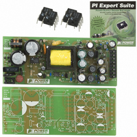
KIT DESIGN ACCELERATOR SET TOP
Manufacturer
Power Integrations
Type
Design Accelerator Kit (DAK)r
Specifications of DAK-32
Contents
Power Supply, Samples, PCB, Software and Documentation
For Use With/related Products
TOP245P
Lead Free Status / RoHS Status
Not applicable / Not applicable
Other names
596-1003


4
thereby allowing the output voltage feedback loop to control the
primary switch current.
Resistor R6 sets the maximum current limit, while R2 and C16 provide
slope compensation. The value of R4 is chosen to ensure that current
does not flow into the M pin, enabling the line sensing features of the
pin. The current out of the M pin falls as the load is reduced until the
M pin inhibit threshold is reached. The supply then operates with a
fixed 25% current limit, lowering the switching frequency to maintain
regulation. This greatly reduces switching losses, maintaining high
standby efficiency and low no-load power consumption.
Key Design Points
• For good cross-regulation, minimize transformer leakage – use
• Shunt regulator (temperature compensated) between 5 V and 3.3 V
• Feedback is taken from both the 3.3 V and 5 V outputs to the refer-
• Primary clamp components VR1, D5, R7, R1 and C2 limit the
• D5 is a slow recovery diode to recover some of the clamp energy.
• Use a Zener clamp for lowest zero load input power consumption.
For the latest updates, visit www.powerint.com
Power Integrations reserves the right to make changes to its products at any time to improve reliability or manufacturability. Power Integrations does not assume any liability arising from the use of any device or circuit described
herein. POWER INTEGRATIONS MAKES NO WARRANTY HEREIN AND SPECIFICALLY DISCLAIMS ALL WARRANTIES INCLUDING, WITHOUT LIMITATIONS, THE IMPLIED WARRANTIES OF MERCHANTABILITY, FITNESS FOR A
PARTICULAR PURPOSE, AND NON-INFRINGEMENT OF THIRD PARTY RIGHTS. The products and applications illustrated herein (transformer construction and circuits external to the
products) may be covered by one or more U.S. and foreign patents or potentially by pending U.S. and foreign patent applications assigned to Power Integrations. A complete list of Power
Integrations' patents may be found at www.powerint.com. Power Integrations grants its customers a license under certain patent rights as set forth at http://www.powerint.com/ip.htm.
The PI logo, TOPSwitch, TinySwitch, LinkSwitch, DPA-Switch, EcoSmart, Clampless, E-Shield, Filterfuse, PI Expert and PI FACTS are trademarks of Power Integrations, Inc. Other
trademarks are property of their respective companies. Copyright 2006, Power Integrations, Inc.
For a complete list of our Worldwide Sales Representatives & Distributors visit our Web site: www.powerint.com
APPLICATIONS HOTLINE
Phone:
Fax:
CUSTOMER SERVICE
Phone:
Fax:
WORLD HEADQUARTERS
San Jose, CA, USA
Phone:
E-mail: usasales@powerint.com
foil for 3.3 V and 5 V outputs; minimize peak primary currents by
designing transformer for continuous conduction mode.
outputs in dotted box on schematic is optional. It is only necessary
where min and max load conditions do not occur simultaneously
on both outputs.
ence (U3) via R9, R11 and R12. The 12 V output is DC stacked on
the 5 V output for enhanced regulation and voltage centering.
leakage inductance induced peak drain voltage spike.
It must be a glass passivated type to guarantee a defined t
DI-55
+1 408-414-9660
+1 408-414-9760
+1 408-414-9665
+1 408-414-9765
+1 408-414-9200
POWER INTEGRATIONS WORLDWIDE SALES SUPPORT LOCATIONS
CHINA (SHANGHAI)
Shanghai, China
Phone:
E-mail: chinasales@powerint.com
CHINA (SHENZHEN)
Shenzhen, China
Phone:
E-mail: chinasales@powerint.com
GERMANY
Munich, Germany
Phone:
E-mail: eurosales@powerint.com
+86-21-6215-5548
+86-755-8379-3243
+49-89-5527-3910
INDIA
Bangalore, India
Phone:
E-mail: indiasales@powerint.com
ITALY
Milano, Italy
Phone:
E-mail: eurosales@powerint.com
JAPAN
Kanagawa, Japan
Phone:
E-mail: japansales@powerint.com
rr
www.powerint.com
.
+91-80-5113-8020
+39-028-928-6000
+81-45-471-1021
Table 1. Transformer Construction Information.
Table 2. Worst Case Output Cross-Regulation - All Outputs Taken
Voltage
-24
(V)
3.3
12
5
Primary Resonant
Winding Details
Winding Order
(Pin Numbers)
Core Material
Inductance
Frequency
KOREA
Seoul, Korea
Phone:
E-mail: koreasales@powerint.com
SINGAPORE
Singapore
Phone:
E-mail: singaporesales@powerint.com
TAIWAN
Taipei, Taiwan
Phone:
E-mail: taiwansales@powerint.com
from Minimum to Maximum Loads.
0.03-0.05
Bobbin
Range
0.3-0.6
0.3-1.2
0.1-0.2
Load
(A)
TRANSFORMER PARAMETERS
+82-2-2016-6610
+65-6358-2160
+886-2-2659-4570
-5 -4 -3 -2 -1
3.3 V/5 V foil: 2T + 1T, 0.12 mm foil
Shield (NC-1), tape, primary
Regulation (%)
EEL25, N67 or equivalent,
Shield 1: 32T, 2 x 32 AWG
Primary: 63T, 2 x 32 AWG
Shield 2: 4T, 4 x 32 AWG
gap for A
Leakage: 80 µH (max.)
foil, (10,11-9-13), -24 V
Primary: 800 µH ±10%
-24 V: 13T, 2 x 32 AWG
tape, shield 2 (13-NC),
(14-10,11), 12 V (12-8)
+12 V: 4T, 4 x 32 AWG
(1-4), tape, bias (5-7),
Bias: 6T, 4 x 32 AWG
300 kHz (minimum)
EUROPE HQ
Farnham, Surrey, United Kingdom
Phone:
E-mail: eurosales@powerint.com
0
7 pin + 7 pin
1
LG
of 202 nH/T
2
+44 (0) 1252-730-140
3
4
5
2
6
7
Related parts for DAK-32
Image
Part Number
Description
Manufacturer
Datasheet
Request
R

Part Number:
Description:
KIT DESIGN ACCELERATOR MODEM
Manufacturer:
Power Integrations
Datasheet:

Part Number:
Description:
KIT REF DES DPA 6.6W DC-DC CONV
Manufacturer:
Power Integrations
Datasheet:

Part Number:
Description:
KIT DESIGN ACCELERATOR POE CONV
Manufacturer:
Power Integrations
Datasheet:

Part Number:
Description:
DESIGN ACCELERATOR KIT XT SWITCH
Manufacturer:
Power Integrations
Datasheet:

Part Number:
Description:
DESIGN ACCELERATOR KIT LP SWITCH
Manufacturer:
Power Integrations
Datasheet:

Part Number:
Description:
KIT DESIGN ACC PEAKSWITCH FAMILY
Manufacturer:
Power Integrations
Datasheet:

Part Number:
Description:
KIT DESIGN ACCELERATOR ADAPTER
Manufacturer:
Power Integrations
Datasheet:

Part Number:
Description:
KIT DESIGN ACCELERATOR ADAPTER
Manufacturer:
Power Integrations
Datasheet:

Part Number:
Description:
KIT DESIGN ACCELERATOR DC-DC
Manufacturer:
Power Integrations
Datasheet:

Part Number:
Description:
KIT DESIGN ACCELERATOR DPA SW
Manufacturer:
Power Integrations
Datasheet: