DAK-34 Power Integrations, DAK-34 Datasheet - Page 38
DAK-34
Manufacturer Part Number
DAK-34
Description
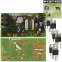
KIT DESIGN ACCELERATOR AC/DC PS
Manufacturer
Power Integrations
Series
TOPSwitch®-GXr
Specifications of DAK-34
Main Purpose
AC/DC, Primary Side
Outputs And Type
1, Isolated
Power - Output
30W
Voltage - Output
12V
Current - Output
2.5A
Voltage - Input
85 ~ 265VAC
Regulator Topology
Flyback
Frequency - Switching
132kHz
Board Type
Bare (Unpopulated) and Fully Populated
Utilized Ic / Part
TOP245
Lead Free Status / RoHS Status
Not applicable / Not applicable
Other names
596-1004


NOTES:
A. For specifications with negative values, a negative temperature coefficient corresponds to an increase in
B. Guaranteed by characterization. Not tested in production.
C. For externally adjusted current limit values, please refer to Figures 54b, 55b and 56b (Current Limit vs. External
D. Breakdown voltage may be checked against minimum BV
E. It is possible to start up and operate TOPSwitch-GX at DRAIN voltages well below 36 V. However, the CONTROL
38
OUTPUT (cont.)
ON-State
Resistance
OFF-State Drain
Leakage Current
Breakdown
Voltage
Rise Time
Fall Time
SUPPLY VOLTAGE CHARACTERISTICS
DRAIN Supply
Voltage
Shunt Regulator
Voltage
Shunt Regulator
Temperature Drift
Control Supply/
Discharge Current
magnitude with increasing temperature, and a positive temperature coefficient corresponds to a decrease in
magnitude with increasing temperature.
Current Limit Resistance) in the Typical Performance Characteristics section. The tolerance specified is only valid
at full current limit.
to but not exceeding minimum BV
pin charging current is reduced, which affects start-up time, auto-restart frequency, and auto-restart duty cycle.
Refer to Figure 68, the characteristic graph on CONTROL pin charge current (I
voltage operation characteristics.
TOP242-250
Parameter
O
11/05
Symbol
V
R
BV
C(SHUNT)
I
I
I
DS(ON)
DSS
CD1
CD2
t
t
R
F
DSS
Output MOSFET
V
DSS
X
SOURCE = 0 V; T
I
I
, V
D
D
.
TOP249
TOP250
Enabled
Measured in a Typical Flyback
= 600 mA
= 700 mA
(Unless Otherwise Specified)
L
V
V
, V
V
L
L
See Note D, T
, V
, V
DS
Converter Application
M
= 0 V
M
M
Output MOSFET
= 560 V; T
V
See Figure 53
Conditions
= Floating; I
= Floating; I
X
See Note E
, V
I
Disabled
C
L
= 4 mA
, V
J
M
= -40 to 125 °C
J
TOP242-245
TOP246-249
= 0 V
J
T
T
= 125 °C
T
T
= 25 °C
J
J
TOP250
J
J
C
C
DSS
= 100 °C
= 100 °C
= 25 °C
= 25 °C
= 4 mA
= 4 mA
specification by ramping the DRAIN pin voltage up
Min
5.60
700
1.0
1.2
1.3
0.3
36
C
) vs. DRAIN voltage for low
Typ
1.30
2.15
1.10
1.85
5.85
100
±50
1.6
2.2
2.4
0.6
50
Max
1.50
2.50
1.28
2.15
6.10
3.65
470
2.5
3.2
1.3
ppm/°C
Units
mA
µA
ns
ns
Ω
V
V
V
Related parts for DAK-34
Image
Part Number
Description
Manufacturer
Datasheet
Request
R

Part Number:
Description:
KIT DESIGN ACCELERATOR MODEM
Manufacturer:
Power Integrations
Datasheet:

Part Number:
Description:
KIT DESIGN ACCELERATOR SET TOP
Manufacturer:
Power Integrations
Datasheet:

Part Number:
Description:
KIT REF DES DPA 6.6W DC-DC CONV
Manufacturer:
Power Integrations
Datasheet:

Part Number:
Description:
KIT DESIGN ACCELERATOR POE CONV
Manufacturer:
Power Integrations
Datasheet:

Part Number:
Description:
DESIGN ACCELERATOR KIT XT SWITCH
Manufacturer:
Power Integrations
Datasheet:

Part Number:
Description:
DESIGN ACCELERATOR KIT LP SWITCH
Manufacturer:
Power Integrations
Datasheet:

Part Number:
Description:
KIT DESIGN ACC PEAKSWITCH FAMILY
Manufacturer:
Power Integrations
Datasheet:

Part Number:
Description:
KIT DESIGN ACCELERATOR ADAPTER
Manufacturer:
Power Integrations
Datasheet:

Part Number:
Description:
KIT DESIGN ACCELERATOR ADAPTER
Manufacturer:
Power Integrations
Datasheet:

Part Number:
Description:
KIT DESIGN ACCELERATOR DC-DC
Manufacturer:
Power Integrations
Datasheet:
