PVG612ASPBF International Rectifier, PVG612ASPBF Datasheet - Page 2
PVG612ASPBF
Manufacturer Part Number
PVG612ASPBF
Description
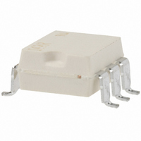
IC RELAY PHOTOVO 60V 2A 6-SMD
Manufacturer
International Rectifier
Series
PVG, HEXFET®r
Datasheet
1.PVG612AS-TPBF.pdf
(5 pages)
Specifications of PVG612ASPBF
Circuit
SPST-NO (1 Form A)
Output Type
AC, DC
On-state Resistance
100 mOhm
Load Current
2A
Voltage - Input
1.2VDC
Voltage - Load
0 ~ 60 V
Mounting Type
Surface Mount
Termination Style
Gull Wing
Package / Case
6-SMD (300 mil)
Brand/series
PVG612A Series
Capacitance, Output
105 pF
Contact Form
SP-NO
Current, Rating
7.5 A
Dielectric Strength
4000 VRMS
Function
Power
Number Of Pins
8
Package Type
DIP
Relay Type
Solid State
Resistance, On-state
100 miiliOhm
Standards
UL
Temperature, Operating, Maximum
+85 °C
Temperature, Operating, Minimum
–40 °C
Termination
Through Hole
Time, Turn-off
0.5 ms
Time, Turn-on
3.5 ms
Voltage, Rating
60 V
Esd Tolerance
- 4000 V Human Body Model - 500 V Machine Model
Load Voltage Max
60V
On State Resistance Max
100mohm
Contact Configuration
SPST-NO
Isolation Voltage
4kV
Forward Current If
25mA
Relay Terminals
SMD
Leaded Process Compatible
Yes
Rohs Compliant
Yes
Load Voltage Rating
60 V
Load Current Rating
4 A
Output Device
MOSFET
Mounting Style
SMD/SMT
Maximum Operating Temperature
+ 85 C
Minimum Operating Temperature
- 40 C
Lead Free Status / RoHS Status
Lead free / RoHS Compliant
Available stocks
Company
Part Number
Manufacturer
Quantity
Price
Company:

Part Number:
PVG612ASPBF
Manufacturer:
AD
Quantity:
1 000
Company:
Part Number:
PVG612ASPBF
Manufacturer:
IR
Quantity:
10


Electrical Specifications (-40°C ≤ T
International Rectifier does not recommend the use of this product in aerospace, avionics, military or life support applications.
Users of this International Rectifier product in such applications assume all risks of such use and indemnify International
Rectifier against all damages resulting from such use.
www.irf.com
INPUT CHARACTERISTICS
Minimum Control Current (see figure 1)
Maximum Control Current for Off-State Resistance @ T
Control Current Range (Caution: current limit input LED, see figure 6)
Maximum Reverse Voltage (1mA max.)
OUTPUT CHARACTERISTICS
Operating Voltage Range
Maximum Continuous Load Current @ T
(see figure 1)
Maximum Pulsed Load Current @ T
Typical Thermal Resistance (Rthja, Junction-to-Ambient)
Maximum On-State Resistance @T
Maximum Off-State Leakage @ 60V, T
Maximum Turn-On Time @T
Maximum Turn-Off Time @T
Typical Output Capacitance @ Vdd=50V, f=1MHz (see figure 2)
GENERAL CHARACTERISTICS
Minimum Dielectric Strength, Input-Output
Minimum Insulation Resistance, Input-Output, @T
Maximum Capacitance, Input-Output
Maximum Pin Soldering Temperature (10 seconds maximum)
Ambient Temperature Range:
For 1A pulsed load, 10mA Control (see figure 4)
For 500mA, 50V
For 500mA, 50V
DC
DC
load, 10mA Control, 10mS pulse width
load, 10mA Control, 10mS pulse width
A
A
=+25°C (see figures 7 & 8)
=+25°C (see figures 7 & 8)
A
A
=+25°C
=+25°C (100 ms @ 10% Duty Cycle)
A
=+25°C
A
= +40°C, 10mA Control
A
≤ +85°C unless otherwise specified)
A
=+25°C, 50%RH, 100V
A Connection
B Connection
C Connection
A Connection
B Connection
C Connection
A Connection
B Connection
C Connection
A Connection
B Connection
C Connection
Operating
Storage
A
= +25°C
DC
-40 to +100
-40 to +85
Limits
Limits
0 to ±60
Limits
5.0 - 25
112.2
4000
+260
15.5
79.1
81.0
10
7.5A
100
105
5.0
0.4
6.0
2.0
2.5
4.0
8.5
1.0
3.5
0.5
1.0
50
35
12
Series PVG612APbF
V
(DC or AC peak)
A (AC or DC)
(AC or DC)
Units
Units
Units
A (DC)
A (DC)
A (DC)
A (DC)
(°C/W)
(°C/W)
(°C/W)
V
mΩ
mΩ
mΩ
mA
mA
mA
ms
ms
µΑ
RMS
pF
pF
°C
Ω
V
2
Related parts for PVG612ASPBF
Image
Part Number
Description
Manufacturer
Datasheet
Request
R

Part Number:
Description:
RELAY PHOTOVO 60V 2AMP 6-DIP
Manufacturer:
International Rectifier
Datasheet:

Part Number:
Description:
Manufacturer:
International Rectifier
Datasheet:

Part Number:
Description:
SCHOTTKY RECTIFIER
Manufacturer:
International Rectifier Corp.
Datasheet:
Part Number:
Description:
SCHOTTKY RECTIFIER
Manufacturer:
International Rectifier Corp.
Datasheet:
Part Number:
Description:
SCHOTTKY RECTIFIER
Manufacturer:
International Rectifier Corp.
Datasheet:
Part Number:
Description:
SCHOTTKY RECTIFIER
Manufacturer:
International Rectifier Corp.
Datasheet:
Part Number:
Description:
SCHOTTKY RECTIFIER
Manufacturer:
International Rectifier Corp.
Datasheet:
Part Number:
Description:
SCHOTTKY RECTIFIER
Manufacturer:
International Rectifier Corp.
Datasheet:
Part Number:
Description:
SCHOTTKY RECTIFIER
Manufacturer:
International Rectifier Corp.
Datasheet:
Part Number:
Description:
SCHOTTKY RECTIFIER
Manufacturer:
International Rectifier Corp.
Datasheet:
Part Number:
Description:
SCHOTTKY RECTIFIER
Manufacturer:
International Rectifier Corp.
Datasheet:
Part Number:
Description:
SCHOTTKY RECTIFIER
Manufacturer:
International Rectifier Corp.
Datasheet:
Part Number:
Description:
SCHOTTKY RECTIFIER
Manufacturer:
International Rectifier Corp.
Datasheet:
Part Number:
Description:
SCHOTTKY RECTIFIER
Manufacturer:
International Rectifier Corp.
Datasheet:
Part Number:
Description:
SCHOTTKY RECTIFIER
Manufacturer:
International Rectifier Corp.
Datasheet: