500X07N2R2CV4T Johanson Dielectrics Inc, 500X07N2R2CV4T Datasheet - Page 6
500X07N2R2CV4T
Manufacturer Part Number
500X07N2R2CV4T
Description
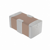
CAP CER X2Y 2.2PF 50V NPO 0402
Manufacturer
Johanson Dielectrics Inc
Series
X2Y®r
Datasheet
1.S-X2Y-MTR.pdf
(8 pages)
Specifications of 500X07N2R2CV4T
Capacitance
2.2pF
Voltage - Rated
50V
Tolerance
±0.25pF
Temperature Coefficient
C0G, NP0
Mounting Type
Surface Mount, MLCC
Operating Temperature
-55°C ~ 125°C
Features
Low Inductance
Applications
Bypass, Decoupling
Package / Case
0402 (1005 Metric)
Size / Dimension
0.045" L x 0.024" W (1.14mm x 0.61mm)
Thickness
0.51mm Max
Lead Free Status / RoHS Status
Lead free / RoHS Compliant
Ratings
-
Lead Spacing
-


S
L
Ceramic capacitors (X2Y and standard MLC types) can be easily damaged when hand soldered. Thermal cracking of the ceramic
body is often invisible even under a microscope. Factors that increase thermal cracking risk:
1. 4 terminals to solder can increase hand-soldering time and temperature exposure
2. Pb-free solders have higher reflow temperatures
3. Low inductance connections to ground are inherently good heat-sinks
A damaged component may exhibit a short circuit immediately and not recover, or may operate with intermittent Insulation Resistance
(IR) levels. If you are not achieving expected results and have followed the other guidelines carefully, check to see you are adhering to
the soldering guidelines below:
• Always pre-heat the PCB and component to within 50°C of solder reflow temperature at 2°C/sec. maximum.
• Use contact-less hand solder tools such as a hot air pencil, IR lamp, etc.
• Avoid over-heating of the ceramic component, temperature limit: 260°C for 20-30 seconds max.
• Use a soldering iron as last resort; 20W max. tip, NO CONTACT with ceramic, limit solder time to 5 seconds max.
A reliable, cost effective prototype PCB reflow soldering process is possible using a household toaster oven. There are several good
procedures available on-line by googling “Toaster Oven Soldering”
O
X2Y capacitors deliver excellent performance in EMI/RFI fi ltering and Power Bypass applications. Physical and electrical placement
on the PCB is critical in achieving good results. A low inductance, dual ground connection is mandatory.
EMI Filter Applications
inductance connections and should be avoided. See detailed application note
PDN / Power Bypass Applications
recommended layout against a poor layout. Because of its long extents from
device terminals to vias, and the wide via separation, the poor layout exhibits
approximately 200% L1 inductance, and 150% L2 inductance compared to
recommended X2Y layouts. See detailed application note
Mounting.
6
OLDER
AB
G
PTIMIZING
X
Y
V
U
Z
E
VALUATION
0.020
0.020
0.024
0.015
0.039
0.064
Fig. 1
P
0402 (X07)
IN
Use of solder mask beneath component is not recommended because of flux/contaminant entrapment.
AD
X2Y P
R
0.51
0.51
0.61
0.38
0.99
1.63
mm
ECOMMENDATIONS
S
OLDERING
ERFORMANCE ON THE
0.035
0.025
0.040
0.020
0.060
0.090
0603 (X14)
IN
Low inductance PCB routing examples are shown in fi gures 1 and 2. Figures 3-5 show unbalanced and high
0.89
0.64
1.02
0.51
1.52
2.29
mm
P
RECAUTIONS
0.050
0.035
0.050
0.022
0.080
0.120
0805 (X15)
Fig. 2
IN
Figures on right compare the X2Y
1.27
0.89
1.27
0.56
2.03
3.05
mm
PCB
www.johanson dielectrics.com
0.065
0.040
0.080
0.040
0.120
0.160
1206 (X18)
IN
1.65
1.02
2.03
1.02
3.05
4.06
X2Y Power Bypass
mm
0.100
0.040
0.080
0.045
0.160
0.160
Fig. 3
1210 (X41)
IN
2.54
1.02
2.03
1.14
4.06
4.06
mm
X2Y EMI FIlter Evaluation and PCB Design
0.100
0.040
0.100
0.045
0.160
0.180
1410 (X44)
IN
2.54
1.02
2.54
1.14
4.06
4.57
mm
Recommended X2Y
Bypass Layout
Fig. 4
0.125
0.040
0.130
0.045
0.190
0.210
1812 (X43)
IN
3.18
1.02
3.30
1.14
4.83
5.33
mm
X
Y
Fig. 5
Z
V
G
V
V
V
Guidelines.
U
Related parts for 500X07N2R2CV4T
Image
Part Number
Description
Manufacturer
Datasheet
Request
R

Part Number:
Description:
CAP CER 1000PF 2000V X7R 1808
Manufacturer:
Johanson Dielectrics Inc
Datasheet:

Part Number:
Description:
CAP CER 3300PF 2000V X7R 1812
Manufacturer:
Johanson Dielectrics Inc
Datasheet:

Part Number:
Description:
Capacitor,Ceramic,2200pF,2KVDC,10-% Tol,10+% Tol,X7R-TC Code,-15,15%-TC,30ppm-TC
Manufacturer:
Johanson Dielectrics Inc
Datasheet:

Part Number:
Description:
CAP CER 1000PF 25V X7R 0402
Manufacturer:
Johanson Dielectrics Inc
Datasheet:
Part Number:
Description:
CAP CER 470PF 50V X7R 0402
Manufacturer:
Johanson Dielectrics Inc
Datasheet:
Part Number:
Description:
CAP CER 22PF 50V NP0 0402
Manufacturer:
Johanson Dielectrics Inc
Datasheet:
Part Number:
Description:
CAP CER 68PF 50V NP0 0402
Manufacturer:
Johanson Dielectrics Inc
Datasheet:
Part Number:
Description:
CAP CER 15PF 50V NP0 0402
Manufacturer:
Johanson Dielectrics Inc
Datasheet:
Part Number:
Description:
CAP CER 4.7PF 50V NP0 0402
Manufacturer:
Johanson Dielectrics Inc
Datasheet:
Part Number:
Description:
CAP CER 150PF 25V NP0 0402
Manufacturer:
Johanson Dielectrics Inc
Datasheet:
Part Number:
Description:
CAP CER 1000PF 2000V X7R 1808
Manufacturer:
Johanson Dielectrics Inc
Datasheet:
Part Number:
Description:
CAP CER 3300PF 2000V X7R 1812
Manufacturer:
Johanson Dielectrics Inc
Datasheet:
Part Number:
Description:
Capacitor,Ceramic,2200pF,2KVDC,10-% Tol,10+% Tol,X7R-TC Code,-15,15%-TC,30ppm-TC
Manufacturer:
Johanson Dielectrics Inc
Datasheet:

Part Number:
Description:
CAP CER 1000PF 2000V X7R 1206
Manufacturer:
Johanson Dielectrics Inc
Datasheet:

Part Number:
Description:
CAP CER 1000PF 500V NP0 1206
Manufacturer:
Johanson Dielectrics Inc
Datasheet: