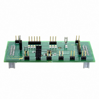
LM27965SQEV National Semiconductor, LM27965SQEV Datasheet

LM27965SQEV
Specifications of LM27965SQEV
Related parts for LM27965SQEV
LM27965SQEV Summary of contents
Page 1
... LED forward voltage, so that effi- ciency is maximized over the input voltage range. The LM27965 is available in National's small 24-pin Leadless Leadframe Package (LLP-24). Typical Application Circuit © 2007 National Semiconductor Corporation Features ■ 91% Peak LED Drive Efficiency ■ No Inductor Required ■ ...
Page 2
Connection Diagram Pin Descriptions Pin #s Pin Names OUT 19, 22 (C1) C1, C2 20, 21 (C2) 12, 13, 14, 15, 16 D5A, D4A, D3A, D2A, D1A D1B, D2B, D3B 3 D1C ...
Page 3
... Absolute Maximum Ratings If Military/Aerospace specified devices are required, please contact the National Semiconductor Sales Office/ Distributors for availability and specifications. V pin voltage IN SCL, SDIO, VIO, RESET pin voltages I Pin Voltages Dxx Continuous Power Dissipation (Note 3) Junction Temperature (T ) J-MAX Storage Temperature Range ...
Page 4
... JA Note 7: Junction-to-ambient thermal resistance is highly dependent on application and board layout. In applications where high maximum power dissipation exists, special care must be paid to thermal dissipation issues in board design. For more information, please refer to National Semiconductor Application Note 1187: Leadless Leadframe Package (AN-1187). Note 8: Min and Max limits are guaranteed by design, test, or statistical analysis. Typical numbers are not guaranteed, but do represent the most likely norm. ...
Page 5
AVG and (AVG-MIN)/AVG. The largest number of the two (worst case) is considered the matching figure for the bank. The matching figure for a given part is considered to be the highest matching figure of the two banks. The typical ...
Page 6
Typical Performance Characteristics 3.6V; R LEDxA LEDxB LED1C SET LED Drive Efficiency vs Input Voltage BankA Current Regulation vs Input Voltage BankC Current Regulation vs Input Voltage www.national.com Unless otherwise specified 16.9kΩ; ...
Page 7
BankB Current Matching vs Input Voltage BankB Diode Current vs Brightness Register Code BankA Diode Current vs Brightness Register Code 20155032 20155027 7 20155026 www.national.com ...
Page 8
Circuit Description OVERVIEW The LM27965 is a white LED driver system based upon an adaptive 3/2× - 1× CMOS charge pump capable of supplying up to 180mA of total output current. With three separately controlled banks of constant current sinks, ...
Page 9
The third byte contains data to write to the selected register. ack = acknowledge (SDIO pulled down by either master or slave chip address, 36h for LM27965 or ...
Page 10
Brightness Level Control Table (BankA and BankB) Brightness Code (hex ...
Page 11
The statement above is a simple example of the LED drive capabilities of the LM27965. The statement contains the key application parameters that are required to validate an LED- drive design using the LM27965: LED current (I of active LEDs ...
Page 12
... National highly recommends a 1:1 ratio between the package and the PCB thermal land. To further enhance thermal con- ductivity, the PCB thermal land may include vias to a ground plane. For more detailed instructions on mounting LLP pack- ages, please refer to National Semiconductor Application Note AN-1187. 12 ...
Page 13
Physical Dimensions inches (millimeters) unless otherwise noted SQA24: 24 Lead LLP X1 = 4.0mm X2 = 4.0mm X3 = 0.8mm 13 www.national.com ...
Page 14
... National Semiconductor and the National Semiconductor logo are registered trademarks of National Semiconductor Corporation. All other brand or product names may be trademarks or registered trademarks of their respective holders. ...


