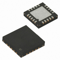
ATTINY84-20MU Atmel, ATTINY84-20MU Datasheet - Page 115

ATTINY84-20MU
Manufacturer Part Number
ATTINY84-20MU
Description
IC MCU AVR 8K FLASH 20MHZ 20-QFN
Manufacturer
Atmel
Series
AVR® ATtinyr
Specifications of ATTINY84-20MU
Core Processor
AVR
Core Size
8-Bit
Speed
20MHz
Connectivity
USI
Peripherals
Brown-out Detect/Reset, POR, PWM, Temp Sensor, WDT
Number Of I /o
12
Program Memory Size
8KB (4K x 16)
Program Memory Type
FLASH
Eeprom Size
512 x 8
Ram Size
512 x 8
Voltage - Supply (vcc/vdd)
2.7 V ~ 5.5 V
Data Converters
A/D 8x10b
Oscillator Type
Internal
Operating Temperature
-40°C ~ 85°C
Package / Case
20-MLF®, QFN
Cpu Family
ATtiny
Device Core
AVR
Device Core Size
8b
Frequency (max)
20MHz
Interface Type
SPI/USI
Total Internal Ram Size
512Byte
# I/os (max)
12
Number Of Timers - General Purpose
2
Operating Supply Voltage (typ)
3.3/5V
Operating Supply Voltage (max)
5.5V
Operating Supply Voltage (min)
2.7V
On-chip Adc
8-chx10-bit
Instruction Set Architecture
RISC
Operating Temp Range
-40C to 85C
Operating Temperature Classification
Industrial
Mounting
Surface Mount
Pin Count
20
Package Type
MLF
Processor Series
ATTINY8x
Core
AVR8
Data Bus Width
8 bit
Data Ram Size
512 B
Maximum Clock Frequency
20 MHz
Number Of Programmable I/os
12
Number Of Timers
2
Operating Supply Voltage
2.7 V to 5.5 V
Maximum Operating Temperature
+ 85 C
Mounting Style
SMD/SMT
3rd Party Development Tools
EWAVR, EWAVR-BL
Development Tools By Supplier
ATAVRDRAGON, ATSTK500, ATSTK600, ATAVRISP2, ATAVRONEKIT
Minimum Operating Temperature
- 40 C
Package
20MLF
Family Name
ATtiny
Maximum Speed
20 MHz
For Use With
ATSTK600 - DEV KIT FOR AVR/AVR32770-1007 - ISP 4PORT ATMEL AVR MCU SPI/JTAGATAVRISP2 - PROGRAMMER AVR IN SYSTEM
Lead Free Status / RoHS Status
Lead free / RoHS Compliant
Available stocks
Company
Part Number
Manufacturer
Quantity
Price
13. Timer/Counter Prescaler
13.1
13.2
8006K–AVR–10/10
Prescaler Reset
External Clock Source
Timer/Counter0 and Timer/Counter1 share the same prescaler module, but the Timer/Counters
can have different prescaler settings. The description below applies to both Timer/Counters. Tn
is used as a general name, n = 0, 1.
The Timer/Counter can be clocked directly by the system clock (by setting the CSn2:0 = 1). This
provides the fastest operation, with a maximum Timer/Counter clock frequency equal to system
clock frequency (f
clock source. The prescaled clock has a frequency of either f
f
The prescaler is free running, i.e., operates independently of the Clock Select logic of the
Timer/CounterCounter, and it is shared by the Timer/Counter Tn. Since the prescaler is not
affected by the Timer/Counter’s clock select, the state of the prescaler will have implications for
situations where a prescaled clock is used. One example of prescaling artifacts occurs when the
timer is enabled and clocked by the prescaler (CSn2:0 = 2, 3, 4, or 5). The number of system
clock cycles from when the timer is enabled to the first count occurs can be from 1 to N+1 sys-
tem clock cycles, where N equals the prescaler divisor (8, 64, 256, or 1024).
The Prescaler Reset can be used for synchronizing the Timer/Counter to program execution.
An external clock source applied to the Tn pin can be used as Timer/Counter clock (clk
Tn pin is sampled once every system clock cycle by the pin synchronization logic. The synchro-
nized (sampled) signal is then passed through the edge detector.
equivalent block diagram of the Tn synchronization and edge detector logic. The registers are
clocked at the positive edge of the internal system clock (
high period of the internal system clock.
Figure 13-1. T0 Pin Sampling
The edge detector generates one clk
= 6) edge it detects. The synchronization and edge detector logic introduces a delay of 2.5 to 3.5
system clock cycles from an edge has been applied to the Tn pin to the counter is updated.
Enabling and disabling of the clock input must be done when Tn has been stable for at least one
system clock cycle, otherwise it is a risk that a false Timer/Counter clock pulse is generated.
Each half period of the external clock applied must be longer than one system clock cycle to
ensure correct sampling. The external clock must be guaranteed to have less than half the sys-
tem clock frequency (f
sampling, the maximum frequency of an external clock it can detect is half the sampling fre-
CLK_I/O
Tn
clk
I/O
/1024.
D
LE
CLK_I/O
Q
ExtClk
Synchronization
). Alternatively, one of four taps from the prescaler can be used as a
D
< f
clk_I/O
Q
/2) given a 50/50% duty cycle. Since the edge detector uses
T
0
pulse for each positive (CSn2:0 = 7) or negative (CSn2:0
clk
CLK_I/O
I/O
D
). The latch is transparent in the
Figure 13-1
Q
/8, f
ATtiny24/44/84
CLK_I/O
Edge Detector
/64, f
shows a functional
CLK_I/O
Tn_sync
(To Clock
Select Logic)
Tn
/256, or
). The
115


