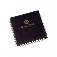
PIC16F877A-I/L Microchip Technology, PIC16F877A-I/L Datasheet - Page 127

PIC16F877A-I/L
Manufacturer Part Number
PIC16F877A-I/L
Description
IC MCU FLASH 8KX14 EE 44PLCC
Manufacturer
Microchip Technology
Series
PIC® 16Fr
Datasheets
1.PIC16F616T-ISL.pdf
(8 pages)
2.PIC16F688T-ISL.pdf
(688 pages)
3.PIC16C770-ISO.pdf
(8 pages)
4.PIC16F873A-ISO.pdf
(234 pages)
5.PIC16F873A-ISO.pdf
(6 pages)
6.PIC16F873A-ISO.pdf
(4 pages)
7.PIC16F873A-ISO.pdf
(6 pages)
8.PIC16F873A-ISO.pdf
(4 pages)
9.PIC16F873A-ISO.pdf
(22 pages)
Specifications of PIC16F877A-I/L
Program Memory Type
FLASH
Program Memory Size
14KB (8K x 14)
Package / Case
44-PLCC
Core Processor
PIC
Core Size
8-Bit
Speed
20MHz
Connectivity
I²C, SPI, UART/USART
Peripherals
Brown-out Detect/Reset, POR, PWM, WDT
Number Of I /o
33
Eeprom Size
256 x 8
Ram Size
368 x 8
Voltage - Supply (vcc/vdd)
4 V ~ 5.5 V
Data Converters
A/D 8x10b
Oscillator Type
External
Operating Temperature
-40°C ~ 85°C
Processor Series
PIC16F
Core
PIC
Data Bus Width
8 bit
Data Ram Size
368 B
Interface Type
I2C/SPI/USART
Maximum Clock Frequency
20 MHz
Number Of Programmable I/os
33
Number Of Timers
3
Operating Supply Voltage
2 V to 5.5 V
Maximum Operating Temperature
+ 85 C
Mounting Style
SMD/SMT
3rd Party Development Tools
52715-96, 52716-328, 52717-734
Development Tools By Supplier
PG164130, DV164035, DV244005, DV164005, PG164120, ICE2000, DM163022, DV164120
Minimum Operating Temperature
- 40 C
On-chip Adc
8-ch x 10-bit
Package
44PLCC
Device Core
PIC
Family Name
PIC16
Maximum Speed
20 MHz
Lead Free Status / RoHS Status
Lead free / RoHS Compliant
For Use With
AC164309 - MODULE SKT FOR PM3 44PLCC444-1001 - DEMO BOARD FOR PICMICRO MCUDVA16XL441 - ADAPTER DEVICE ICE 44PLCC309-1040 - ADAPTER 44-PLCC ZIF TO 40-DIP309-1039 - ADAPTER 44-PLCC TO 40-DIPDV007003 - PROGRAMMER UNIVERSAL PROMATE II
Lead Free Status / Rohs Status
Lead free / RoHS Compliant
Other names
PIC16F877AI/L
Available stocks
Company
Part Number
Manufacturer
Quantity
Price
Company:
Part Number:
PIC16F877A-I/L
Manufacturer:
NEC
Quantity:
1 600
Company:
Part Number:
PIC16F877A-I/L
Manufacturer:
Microchip Technology
Quantity:
10 000
Company:
Part Number:
PIC16F877A-I/LG
Manufacturer:
Microchip Technology
Quantity:
10 000
TABLE 10-10: REGISTERS ASSOCIATED WITH SYNCHRONOUS SLAVE TRANSMISSION
10.4.2
The operation of the Synchronous Master and Slave
modes is identical, except in the case of the Sleep
mode. Bit SREN is a “don't care” in Slave mode.
If receive is enabled by setting bit CREN prior to the
SLEEP instruction, then a word may be received during
Sleep. On completely receiving the word, the RSR reg-
ister will transfer the data to the RCREG register and if
enable bit RCIE bit is set, the interrupt generated will
wake the chip from Sleep. If the global interrupt is
enabled, the program will branch to the interrupt vector
(0004h).
TABLE 10-11: REGISTERS ASSOCIATED WITH SYNCHRONOUS SLAVE RECEPTION
2003 Microchip Technology Inc.
0Bh, 8Bh,
10Bh,18Bh
0Ch
18h
19h
8Ch
98h
99h
Legend:
Note 1:
0Bh, 8Bh,
10Bh,18Bh
0Ch
18h
1Ah
8Ch
98h
99h
Legend:
Note 1:
Address
Address
x = unknown, - = unimplemented, read as ‘0’. Shaded cells are not used for synchronous slave transmission.
Bits PSPIE and PSPIF are reserved on 28-pin devices; always maintain these bits clear.
x = unknown, - = unimplemented, read as ‘0’. Shaded cells are not used for synchronous slave reception.
Bits PSPIE and PSPIF are reserved on 28-pin devices, always maintain these bits clear.
USART SYNCHRONOUS SLAVE
RECEPTION
INTCON
PIR1
RCSTA
RCREG
PIE1
TXSTA
SPBRG
INTCON
PIR1
RCSTA
TXREG
PIE1
TXSTA
SPBRG
Name
Name
USART Receive Register
Baud Rate Generator Register
PSPIF
PSPIE
USART Transmit Register
Baud Rate Generator Register
PSPIF
PSPIE
CSRC
SPEN
SPEN
CSRC
Bit 7
Bit 7
GIE
GIE
(1)
(1)
(1)
(1)
ADIE
PEIE
ADIF
Bit 6
RX9
TX9
PEIE
ADIF
ADIE
Bit 6
RX9
TX9
TMR0IE
SREN
TXEN
TMR0IE
RCIE
RCIF
Bit 5
SREN
TXEN
RCIE
RCIF
Bit 5
CREN ADDEN
SYNC
INTE
Bit 4
TXIF
TXIE
CREN ADDEN
SYNC
INTE
Bit 4
TXIF
TXIE
SSPIF
SSPIE
RBIE
Bit 3
SSPIE
SSPIF
RBIE
Bit 3
—
—
When setting up a Synchronous Slave Reception,
follow these steps:
1.
2.
3.
4.
5.
6.
7.
8.
9.
TMR0IF
CCP1IF TMR2IF TMR1IF 0000 0000 0000 0000
CCP1IE TMR2IE TMR1IE 0000 0000 0000 0000
BRGH
TMR0IF
CCP1IF TMR2IF TMR1IF 0000 0000 0000 0000
CCP1IE TMR2IE TMR1IE 0000 0000 0000 0000
FERR
Bit 2
BRGH
FERR
Bit 2
Enable the synchronous master serial port by
setting bits SYNC and SPEN and clearing bit
CSRC.
If interrupts are desired, set enable bit RCIE.
If 9-bit reception is desired, set bit RX9.
To enable reception, set enable bit CREN.
Flag bit RCIF will be set when reception is
complete and an interrupt will be generated if
enable bit RCIE was set.
Read the RCSTA register to get the ninth bit (if
enabled) and determine if any error occurred
during reception.
Read the 8-bit received data by reading the
RCREG register.
If any error occurred, clear the error by clearing
bit CREN.
If using interrupts, ensure that GIE and PEIE
(bits 7 and 6) of the INTCON register are set.
OERR
TRMT
OERR
INTF
TRMT
Bit 1
INTF
Bit 1
PIC16F87XA
RX9D
TX9D
RX9D
TX9D
Bit 0
R0IF
Bit 0
R0IF
0000 000x 0000 000x
0000 0000 0000 0000
0000 -010 0000 -010
0000 0000 0000 0000
0000 000x
0000 000x 0000 000x
0000 0000 0000 0000
0000 -010 0000 -010
0000 0000 0000 0000
0000 000x 0000 000u
POR, BOR
POR, BOR
Value on:
Value on:
DS39582B-page 125
0000 000u
Value on
Value on
all other
all other
Resets
Resets


