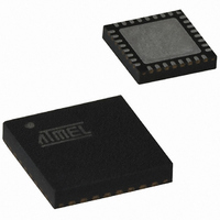
ATTINY461V-10MU Atmel, ATTINY461V-10MU Datasheet - Page 154

ATTINY461V-10MU
Manufacturer Part Number
ATTINY461V-10MU
Description
IC MCU AVR 4K FLASH 10MHZ 32-QFN
Manufacturer
Atmel
Series
AVR® ATtinyr
Specifications of ATTINY461V-10MU
Core Processor
AVR
Core Size
8-Bit
Speed
10MHz
Connectivity
USI
Peripherals
Brown-out Detect/Reset, POR, PWM, WDT
Number Of I /o
16
Program Memory Size
4KB (2K x 16)
Program Memory Type
FLASH
Eeprom Size
256 x 8
Ram Size
256 x 8
Voltage - Supply (vcc/vdd)
1.8 V ~ 5.5 V
Data Converters
A/D 11x10b
Oscillator Type
Internal
Operating Temperature
-40°C ~ 85°C
Package / Case
32-VQFN Exposed Pad, 32-HVQFN, 32-SQFN, 32-DHVQFN
Processor Series
ATTINY4x
Core
AVR8
Data Bus Width
8 bit
Data Ram Size
256 B
Interface Type
2-Wire, SPI, USI
Maximum Clock Frequency
10 MHz
Number Of Programmable I/os
16
Number Of Timers
2
Operating Supply Voltage
1.8 V to 5.5 V
Maximum Operating Temperature
+ 85 C
Mounting Style
SMD/SMT
Minimum Operating Temperature
- 40 C
On-chip Adc
10 bit, 16 Channel
Package
32MLF EP
Device Core
AVR
Family Name
ATtiny
Maximum Speed
10 MHz
For Use With
ATSTK600 - DEV KIT FOR AVR/AVR32ATAVRBC100 - REF DESIGN KIT BATTERY CHARGER770-1007 - ISP 4PORT ATMEL AVR MCU SPI/JTAG
Lead Free Status / RoHS Status
Lead free / RoHS Compliant
Available stocks
Company
Part Number
Manufacturer
Quantity
Price
Company:
Part Number:
ATTINY461V-10MUR
Manufacturer:
Atmel
Quantity:
9 818
15.11.2
15.11.3
15.12 Temperature Measurement
154
ATtiny261/461/861
Unipolar Differential Conversion
Bipolar Differential Conversion
0x3FF represents the selected voltage reference minus one LSB. The result is presented in one-
sided form, from 0x3FF to 0x000.
If differential channels and an unipolar input mode are used, the result is
where V
and V
157). The voltage on the positive pin must always be larger than the voltage on the negative pin
or otherwise the voltage difference is saturated to zero. The result is presented in one-sided
form, from 0x000 (0d) to 0x3FF (+1023d). The GAIN is either 1x, 8x, 20x or 32x.
As default the ADC converter operates in the unipolar input mode, but the bipolar input mode
can be selected by writting the BIN bit in the ADCSRB to one. In the bipolar input mode two-
sided voltage differences are allowed and thus the voltage on the negative input pin can also be
larger than the voltage on the positive input pin. If differential channels and a bipolar input mode
are used, the result is
where V
and V
0x200 (-512d) through 0x000 (+0d) to 0x1FF (+511d). The GAIN is either 1x, 8x, 20x or 32x.
However, if the signal is not bipolar by nature (9 bits + sign as the 10th bit), this scheme loses
one bit of the converter dynamic range. Then, if the user wants to perform the conversion with
the maximum dynamic range, the user can perform a quick polarity check of the result and use
the unipolar differential conversion with selectable differential input pair. When the polarity check
is performed, it is sufficient to read the MSB of the result (ADC9 in ADCH). If the bit is one, the
result is negative, and if this bit is zero, the result is positive.
The temperature measurement is based on an on-chip temperature sensor that is coupled to a
single ended ADC11 channel. Selecting the ADC11 channel by writing the MUX5:0 bits in
ADMUX register to “111111” enables the temperature sensor. The internal 1.1V voltage refer-
ence must also be selected for the ADC voltage reference source in the temperature sensor
measurement. When the temperature sensor is enabled, the ADC converter can be used in sin-
gle conversion mode to measure the voltage over the temperature sensor.
The measured voltage has a linear relationship to the temperature as described in
The sensitivity is approximately 1 LSB /
ibration. Typically, the measurement accuracy after a single temperature calibration is ±
REF
REF
POS
POS
the selected voltage reference. The result is presented in two’s complement form, from
the selected voltage reference (see
is the voltage on the positive input pin, V
is the voltage on the positive input pin, V
ADC
ADC
=
=
(
------------------------------------------------------- - GAIN
(
---------------------------------------------------- - GAIN
V
V
POS
POS
°
C and the accuracy depends on the method of user cal-
–
–
V
V
V
V
REF
Table 15-3 on page 155
REF
NEG
NEG
) 1024
) 512
⋅
⋅
NEG
NEG
⋅
the voltage on the negative input pin,
the voltage on the negative input pin,
⋅
and
Table 15-4 on page
2588E–AVR–08/10
Table 15-2
10°
C,


