PIC24FJ256DA210-I/PT Microchip Technology, PIC24FJ256DA210-I/PT Datasheet - Page 73
PIC24FJ256DA210-I/PT
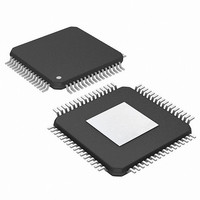
Manufacturer Part Number
PIC24FJ256DA210-I/PT
Description
MCU PIC 16BIT FLASH 256K 100TQFP
Manufacturer
Microchip Technology
Series
PIC® 24Fr
Specifications of PIC24FJ256DA210-I/PT
Core Size
16-Bit
Program Memory Size
256KB (85.5K x 24)
Core Processor
PIC
Speed
32MHz
Connectivity
I²C, IrDA, SPI, UART/USART, USB OTG
Peripherals
Brown-out Detect/Reset, GFX, LVD, POR, PWM, WDT
Number Of I /o
84
Program Memory Type
FLASH
Ram Size
96K x 8
Voltage - Supply (vcc/vdd)
2.2 V ~ 3.6 V
Data Converters
A/D 24x10b
Oscillator Type
Internal
Operating Temperature
-40°C ~ 85°C
Package / Case
100-TFQFP
Controller Family/series
PIC24
No. Of I/o's
84
Ram Memory Size
96KB
Cpu Speed
32MHz
No. Of Timers
5
Interface
I2C, SPI, UART, USB
Embedded Interface Type
I2C, SPI, UART, USB
Rohs Compliant
Yes
Processor Series
PIC24FJ
Core
PIC
Data Bus Width
16 bit
Data Ram Size
96 KB
Interface Type
UART, SPI, USB, I2C, RS-485, RS-232
Maximum Clock Frequency
32 MHz
Number Of Programmable I/os
23
Number Of Timers
5
Operating Supply Voltage
3.6 V
Maximum Operating Temperature
+ 85 C
Mounting Style
SMD/SMT
3rd Party Development Tools
52713-733, 52714-737, 53276-922, EWDSPIC
Development Tools By Supplier
PG164130, DV164035, DV244005, DV164005, AC164127-4, AC164127-6, AC164139, DM240001, DM240312, DV164039
Minimum Operating Temperature
- 40 C
Lead Free Status / RoHS Status
Lead free / RoHS Compliant
Eeprom Size
-
Lead Free Status / Rohs Status
Details
Available stocks
Company
Part Number
Manufacturer
Quantity
Price
Company:

Part Number:
PIC24FJ256DA210-I/PT
Manufacturer:
Microchip Technology
Quantity:
10 000
Part Number:
PIC24FJ256DA210-I/PT
Manufacturer:
MICROCHIP/微芯
Quantity:
20 000


4.2.5.2
In order to write data to EDS space, such as in EDS
reads, an Address Pointer is set up by loading the
required EDS page number into the DSWPAG register,
and assigning the offset address to one of the W regis-
ters. Once the above assignment is done, then the
FIGURE 4-6:
When the MSBs of EA is ‘1’, the lower 9 bits of
DSWPAG are concatenated to the lower 15 bits of EA
to form a 24-bit EDS address for write operations.
Example 4-2 shows how to write a byte, word and dou-
ble-word to EDS.
EXAMPLE 4-2:
2010 Microchip Technology Inc.
; Set the EDS page where the data to be written
;Write a byte to the selected location
;Write a word to the selected location
;Write a Double - word to the selected location
mov
mov
mov
bset
mov
mov
mov.b
mov.b
mov
mov
mov
mov
mov.d
Data Write into EDS Space
#0x0002 , w0
w0 , DSWPAG
#0x0800 ,
w1 , #15
#0x00A5 , w2
#0x003C , w3
w2 , [w1++]
w3 , [w1++]
#0x1234
w2 , [w1]
#0x1122 , w2
#0x4455 , w3
w2 , [w1]
8
EDS ADDRESS GENERATION FOR WRITE OPERATIONS
EDS WRITE CODE IN ASSEMBLY
, w2
DSWPAG Reg
w1
9 Bits
;page 2 is selected for write
;select the location (0x800) to be written
;set the MSB of the base address, enable EDS mode
;write High byte
;
;
;2 EDS writes
Select
;write Low byte
0
1
PIC24FJ256DA210 FAMILY
24-Bit EA
EDS window is enabled by setting bit 15 of the working
register, assigned with the offset address, and the
accessed location can be written.
Figure 4-2 illustrates how the EDS space address is
generated for write operations.
Wn
15 Bits
Wn<0> is Byte Select
DS39969B-page 73
Related parts for PIC24FJ256DA210-I/PT
Image
Part Number
Description
Manufacturer
Datasheet
Request
R

Part Number:
Description:
Manufacturer:
Microchip Technology Inc.
Datasheet:
Part Number:
Description:
Manufacturer:
Microchip Technology Inc.
Datasheet:
Part Number:
Description:
Manufacturer:
Microchip Technology Inc.
Datasheet:
Part Number:
Description:
Manufacturer:
Microchip Technology Inc.
Datasheet:
Part Number:
Description:
Manufacturer:
Microchip Technology Inc.
Datasheet:
Part Number:
Description:
Manufacturer:
Microchip Technology Inc.
Datasheet:
Part Number:
Description:
Manufacturer:
Microchip Technology Inc.
Datasheet:
Part Number:
Description:
Manufacturer:
Microchip Technology Inc.
Datasheet: