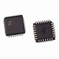
Z86E3116VSG Zilog, Z86E3116VSG Datasheet - Page 25

Z86E3116VSG
Manufacturer Part Number
Z86E3116VSG
Description
IC MICROCONTROLLER 2K 28-PLCC
Manufacturer
Zilog
Series
Z8®r
Datasheet
1.Z86E4001ZDV.pdf
(64 pages)
Specifications of Z86E3116VSG
Core Processor
Z8
Core Size
8-Bit
Speed
16MHz
Peripherals
POR, WDT
Number Of I /o
24
Program Memory Size
2KB (2K x 8)
Program Memory Type
OTP
Ram Size
125 x 8
Voltage - Supply (vcc/vdd)
3.5 V ~ 5.5 V
Oscillator Type
Internal
Operating Temperature
0°C ~ 70°C
Package / Case
28-PLCC
Processor Series
Z86E3xx
Core
Z8
Data Bus Width
8 bit
Data Ram Size
125 B
Maximum Clock Frequency
16 MHz
Number Of Programmable I/os
24
Number Of Timers
2
Operating Supply Voltage
3.5 V to 5.5 V
Maximum Operating Temperature
+ 70 C
Mounting Style
SMD/SMT
Minimum Operating Temperature
0 C
Lead Free Status / RoHS Status
Lead free / RoHS Compliant
Eeprom Size
-
Data Converters
-
Connectivity
-
Lead Free Status / Rohs Status
Details
Available stocks
Company
Part Number
Manufacturer
Quantity
Price
Zilog
Port 0 (P07–P00). Port 0 is an 8-bit, bidirectional, CMOS-
compatible I/O port. These eight I/O lines can be config-
ured under software control as a nibble I/O port, or as an
address port for interfacing external memory. The input
buffers are Schmitt-triggered and nibble programmed. Ei-
ther nibble output that can be globally programmed as
push-pull or open-drain. Low EMI output buffers can be
globally programmed by the software. Port 0 can be placed
under handshake control. In Handshake Mode, Port 3
lines P32 and P35 are used as handshake control lines.
The handshake direction is determined by the configura-
tion (input or output) assigned to Port 0's upper nibble. The
lower nibble must have the same direction as the upper
nibble.
For external memory references, Port 0 provides address
bits A11–A8 (lower nibble) or A15–A8 (lower and upper
DS97Z8X0502
OEN
Out
Open-Drain
In
1.5
2.3V Hysteresis
Figure 18. Port 0 Configuration
P R E L I M I N A R Y
4
4
R
nibble) depending on the required address space. If the
address range requires 12 bits or less, the upper nibble of
Port 0 can be programmed independently as I/O while the
lower nibble is used for addressing. If one or both nibbles
are needed for I/O operation, they must be configured by
writing to the Port 0 mode register. In ROMless mode, after
a hardware reset, Port 0 is configured as address lines
A15–A8, and extended timing is set to accommodate slow
memory access. The initialization routine can include re-
configuration to eliminate this extended timing mode. In
ROM mode, Port 0 is defined as input after reset.
Port 0 can be set in the High-Impedance Mode if selected
as an address output state, along with Port 1 and the con-
trol signals AS, DS, and R/W (Figure 18).
500 k
Handshake Controls
/DAV0 and RDY0
(P32 and P35)
Port 0 (I/O)
Auto Latch
Z8 4K OTP Microcontroller
PAD
Z86E30/E31/E40
25
1


