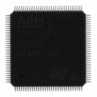
STR910FAW32X6 STMicroelectronics, STR910FAW32X6 Datasheet - Page 39

STR910FAW32X6
Manufacturer Part Number
STR910FAW32X6
Description
MCU 256KB FLASH 64K RAM 128LQFP
Manufacturer
STMicroelectronics
Series
STR9r
Datasheet
1.STEVAL-IFW001V1.pdf
(102 pages)
Specifications of STR910FAW32X6
Core Processor
ARM9
Core Size
32-Bit
Speed
96MHz
Connectivity
CAN, EBI/EMI, I²C, IrDA, Microwire, SPI, SSI, SSP, UART/USART
Peripherals
Brown-out Detect/Reset, DMA, POR, PWM, WDT
Number Of I /o
80
Program Memory Size
256KB (256K x 8)
Program Memory Type
FLASH
Ram Size
64K x 8
Voltage - Supply (vcc/vdd)
1.65 V ~ 2 V
Data Converters
A/D 8x10b
Oscillator Type
Internal
Operating Temperature
-40°C ~ 85°C
Package / Case
128-LQFP
Processor Series
STR910x
Core
ARM966E-S
Data Bus Width
16 bit, 32 bit
Data Ram Size
64 KB
Interface Type
CAN/I2C/IrDA/SSP/UART
Maximum Clock Frequency
96 MHz
Number Of Programmable I/os
80
Number Of Timers
4
Maximum Operating Temperature
+ 85 C
Mounting Style
SMD/SMT
3rd Party Development Tools
EWARM, EWARM-BL, MCBSTR9, MCBSTR9U, MCBSTR9UME, MDK-ARM, RL-ARM, ULINK2
Development Tools By Supplier
STR9-COMSTICK, STR910-EVAL, STR91X-SK/HIT, STR91X-SK/IAR, STR91X-SK/KEI, STR91X-SK/RAI, STR9-DK/RAIS, STR91X-DK/IAR, STX-PRO/RAIS, STR912-D/RAIS, STR79-RVDK/CPP, STR79-RVDKCPP/9, STR79-RVDK, STR79-RVDK/9, STR9-RVDK/BAS, STR79-RVDK/UPG
Minimum Operating Temperature
- 40 C
On-chip Adc
8-ch x 10-bit
For Use With
497-8268 - BOARD EVAL FOR EVAL-STR910MCBSTR9UME - BOARD EVAL MCBSTR9 + ULINK-MEMCBSTR9U - BOARD EVAL MCBSTR9 + ULINK2MCBSTR9 - BOARD EVAL STM STR9 SERIES497-5067 - BOARD EVAL FOR STR910 FAMILY497-5066 - KIT STARTER KEIL FOR STR910497-5065 - KIT STARTER IAR KICKSTART STR912497-5064 - KIT STARTER FOR STR910 FAMILY497-5046 - KIT TOOL FOR ST7/UPSD/STR7 MCU
Lead Free Status / RoHS Status
Lead free / RoHS Compliant
Eeprom Size
-
Lead Free Status / Rohs Status
Lead free / RoHS Compliant
Other names
497-6276
Available stocks
Company
Part Number
Manufacturer
Quantity
Price
Company:
Part Number:
STR910FAW32X6
Manufacturer:
LATTICE
Quantity:
95
Company:
Part Number:
STR910FAW32X6
Manufacturer:
STMicroelectronics
Quantity:
10 000
STR91xFAxxx
EMI_BWR_WRLn is the data write strobe, and the output on pin EMI_RDn is the data read
strobe.
●
●
8-bit non-multiplexed data mode
bits of address are output on ports 7 and 9. The output signal on pin EMI_BWR_BWLn
is the data write strobe and the output on pin EMI_RDn is the data read strobe.
Burst Mode Support (LFBGA package only): The EMI bus supports synchronized
burst read and write bus cycle in multiplexed and non-multiplexed mode. The additional
EMI signals in the LFBGA package that support the burst mode are:
–
–
–
–
–
By defining the bus parameters such as burst length, burst type, read and write timings
in the EMI control registers, the EMI bus is able to interface to standard burst memory
devices. The burst timing specification and waveform will be provided in the next data
sheet release
EMI_BCLK -the bus clock output. The EMI_BCLK has the same frequency or half
of that of the HCLK and can be disabled by the user
EMI_WAITn - the not ready or wait input signal for synchronous access
EMI_BAAn - burst address advance or burst enable signal
EMI_WEn - write enable signal
EMI_UBn, EMI_LBn - upper byte and lower byte enable signals. These two signals
share the same pins as the EMI_WRLn and EMI_WRHn and are user configurable
through the EMI register.
Doc ID 13495 Rev 6
(Figure
6): Eight bits of data are on port 8, while 16
Functional overview
39/102


