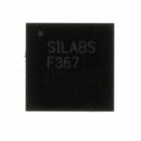
C8051F367-GM Silicon Laboratories Inc, C8051F367-GM Datasheet - Page 26

C8051F367-GM
Manufacturer Part Number
C8051F367-GM
Description
IC 8051 MCU 32K FLASH 28-QFN
Manufacturer
Silicon Laboratories Inc
Series
C8051F36xr
Specifications of C8051F367-GM
Program Memory Type
FLASH
Program Memory Size
32KB (32K x 8)
Package / Case
28-QFN
Core Processor
8051
Core Size
8-Bit
Speed
50MHz
Connectivity
SMBus (2-Wire/I²C), SPI, UART/USART
Peripherals
POR, PWM, Temp Sensor, WDT
Number Of I /o
25
Ram Size
1K x 8
Voltage - Supply (vcc/vdd)
2.7 V ~ 3.6 V
Data Converters
A/D 17x10b; D/A 1x10b
Oscillator Type
Internal
Operating Temperature
-40°C ~ 85°C
Processor Series
C8051F3x
Core
8051
Data Bus Width
8 bit
Data Ram Size
1 KB
Interface Type
I2C/SMBus/SPI/UART
Maximum Clock Frequency
50 MHz
Number Of Programmable I/os
25
Number Of Timers
4
Maximum Operating Temperature
+ 85 C
Mounting Style
SMD/SMT
3rd Party Development Tools
KSK-SL-TOOLSTICK, PK51, CA51, A51, ULINK2
Development Tools By Supplier
C8051F360DK
Minimum Operating Temperature
- 40 C
On-chip Adc
21-ch x 10-bit
On-chip Dac
1-ch x 10-bit
Package
28QFN EP
Device Core
8051
Family Name
C8051F36x
Maximum Speed
50 MHz
Operating Supply Voltage
3 V
Lead Free Status / RoHS Status
Lead free / RoHS Compliant
For Use With
770-1006 - ISP 4PORT FOR SILABS C8051F MCU336-1410 - KIT DEV FOR C8051F360 FAMILY
Eeprom Size
-
Lead Free Status / Rohs Status
Lead free / RoHS Compliant
Other names
336-1649
Available stocks
Company
Part Number
Manufacturer
Quantity
Price
Company:
Part Number:
C8051F367-GM
Manufacturer:
Silicon Labs
Quantity:
135
- Current page: 26 of 288
- Download datasheet (3Mb)
C8051F360/1/2/3/4/5/6/7/8/9
The Digital Crossbar allows mapping of internal digital system resources to Port I/O pins. (See Figure 1.8.)
On-chip counter/timers, serial buses, HW interrupts, comparator output, and other digital signals in the
controller can be configured to appear on the Port I/O pins specified in the Crossbar Control registers. This
allows the user to select the exact mix of general purpose Port I/O and digital resources needed for the
particular application.
1.5.
The C8051F36x Family includes an SMBus/I
configuration, and an Enhanced SPI interface. Each of the serial buses is fully implemented in hardware
and makes extensive use of the CIP-51's interrupts, thus requiring very little CPU intervention.
1.6.
An on-chip Programmable Counter/Timer Array (PCA) is included in addition to the four 16-bit general pur-
pose counter/timers. The PCA consists of a dedicated 16-bit counter/timer time base with three program-
mable capture/compare modules. The PCA clock is derived from one of six sources: the system clock
divided by 12, the system clock divided by 4, Timer 0 overflows, an External Clock Input (ECI), the system
clock, or the external oscillator clock source divided by 8. The external clock source selection is useful for
26
Highest
Priority
Lowest
Priority
Serial Ports
Programmable Counter Array
SYSCLK
Outputs
SMBus
T0, T1
UART
P0
P1
P2
P3
CP0
CP1
PCA
SPI
(P3.0-P3.7)
(P0.0-P0.7)
(P1.0-P1.7)
(P2.0-P2.7)
Figure 1.8. Digital Crossbar Diagram (Port 0 to Port 3)
2
4
2
4
7
2
8
8
8
8
PnSKIP Registers
XBR0, XBR1,
Crossbar
Decoder
Priority
Digital
2
C interface, a full-duplex UART with enhanced baud rate
Rev. 1.0
8
8
8
8
P1MASK, P1MATCH,
P0MASK, P0MATCH
P2MASK, P2MATCH
Registers
Cells
Cells
Cells
Cell
I/O
I/O
I/O
I/O
P0
P1
P2
P3
PnMDIN Registers
PnMDOUT,
3.5–3.7 available on
C8051F360/3
P0.0
P0.7
P1.0
P1.7
P2.0
P2.7
P3.0
P3.7
C8051F360/1/3/4/6/8
3.1–3.4 available on
Related parts for C8051F367-GM
Image
Part Number
Description
Manufacturer
Datasheet
Request
R
Part Number:
Description:
SMD/C°/SINGLE-ENDED OUTPUT SILICON OSCILLATOR
Manufacturer:
Silicon Laboratories Inc
Part Number:
Description:
Manufacturer:
Silicon Laboratories Inc
Datasheet:
Part Number:
Description:
N/A N/A/SI4010 AES KEYFOB DEMO WITH LCD RX
Manufacturer:
Silicon Laboratories Inc
Datasheet:
Part Number:
Description:
N/A N/A/SI4010 SIMPLIFIED KEY FOB DEMO WITH LED RX
Manufacturer:
Silicon Laboratories Inc
Datasheet:
Part Number:
Description:
N/A/-40 TO 85 OC/EZLINK MODULE; F930/4432 HIGH BAND (REV E/B1)
Manufacturer:
Silicon Laboratories Inc
Part Number:
Description:
EZLink Module; F930/4432 Low Band (rev e/B1)
Manufacturer:
Silicon Laboratories Inc
Part Number:
Description:
I°/4460 10 DBM RADIO TEST CARD 434 MHZ
Manufacturer:
Silicon Laboratories Inc
Part Number:
Description:
I°/4461 14 DBM RADIO TEST CARD 868 MHZ
Manufacturer:
Silicon Laboratories Inc
Part Number:
Description:
I°/4463 20 DBM RFSWITCH RADIO TEST CARD 460 MHZ
Manufacturer:
Silicon Laboratories Inc
Part Number:
Description:
I°/4463 20 DBM RADIO TEST CARD 868 MHZ
Manufacturer:
Silicon Laboratories Inc
Part Number:
Description:
I°/4463 27 DBM RADIO TEST CARD 868 MHZ
Manufacturer:
Silicon Laboratories Inc
Part Number:
Description:
I°/4463 SKYWORKS 30 DBM RADIO TEST CARD 915 MHZ
Manufacturer:
Silicon Laboratories Inc
Part Number:
Description:
N/A N/A/-40 TO 85 OC/4463 RFMD 30 DBM RADIO TEST CARD 915 MHZ
Manufacturer:
Silicon Laboratories Inc
Part Number:
Description:
I°/4463 20 DBM RADIO TEST CARD 169 MHZ
Manufacturer:
Silicon Laboratories Inc


