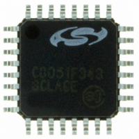
C8051F343-GQ Silicon Laboratories Inc, C8051F343-GQ Datasheet - Page 218

C8051F343-GQ
Manufacturer Part Number
C8051F343-GQ
Description
IC 8051 MCU FLASH 32K 32LQFP
Manufacturer
Silicon Laboratories Inc
Series
C8051F34xr
Specifications of C8051F343-GQ
Program Memory Type
FLASH
Program Memory Size
32KB (32K x 8)
Package / Case
32-LQFP
Core Processor
8051
Core Size
8-Bit
Speed
48MHz
Connectivity
SMBus (2-Wire/I²C), SPI, UART/USART, USB
Peripherals
Brown-out Detect/Reset, POR, PWM, Temp Sensor, WDT
Number Of I /o
25
Ram Size
2.25K x 8
Voltage - Supply (vcc/vdd)
2.7 V ~ 3.6 V
Data Converters
A/D 21x10b
Oscillator Type
Internal
Operating Temperature
-40°C ~ 85°C
Processor Series
C8051F3x
Core
8051
Data Bus Width
8 bit
Data Ram Size
2304 B
Interface Type
I2C, SMBus, SPI, UART, USB
Maximum Clock Frequency
48 MHz
Number Of Programmable I/os
25
Number Of Timers
4
Operating Supply Voltage
2.7 V to 5.25 V
Maximum Operating Temperature
+ 85 C
Mounting Style
SMD/SMT
3rd Party Development Tools
KSK-SL-F34X, KSK-SL-TOOLSTICK, PK51, CA51, A51, ULINK2
Development Tools By Supplier
C8051F340DK
Minimum Operating Temperature
- 40 C
On-chip Adc
10 bit, 17 Channel
Package
32LQFP
Device Core
8051
Family Name
C8051F34x
Maximum Speed
48 MHz
Data Rom Size
128 B
A/d Bit Size
10 bit
A/d Channels Available
17
Height
1.4 mm
Length
7 mm
Supply Voltage (max)
3.6 V
Supply Voltage (min)
2.7 V
Width
7 mm
Lead Free Status / RoHS Status
Lead free / RoHS Compliant
For Use With
336-1748 - ADAPTER TOOLSTICK FOR C8051F34X770-1006 - ISP 4PORT FOR SILABS C8051F MCU
Eeprom Size
-
Lead Free Status / Rohs Status
Lead free / RoHS Compliant
Other names
336-1301
Available stocks
Company
Part Number
Manufacturer
Quantity
Price
Company:
Part Number:
C8051F343-GQ
Manufacturer:
Silicon Laboratories Inc
Quantity:
10 000
Company:
Part Number:
C8051F343-GQR
Manufacturer:
Silicon Laboratories Inc
Quantity:
10 000
C8051F340/1/2/3/4/5/6/7/8/9/A/B/C/D
218
Bit7:
Bit6:
Bit5:
Bit4:
Bit3:
Bit2:
Bit1:
Bit0:
OVR1
R/W
Bit7
OVR1: Receive FIFO Overrun Flag.
This bit is used to indicate a receive FIFO overrun condition.
0: Receive FIFO Overrun has not occurred.
1: Receive FIFO Overrun has occurred (an incoming character was discarded due to a full
FIFO).
This bit must be cleared to ‘0’ by software.
PERR1: Parity Error Flag.
When parity is enabled, this bit is used to indicate that a parity error has occurred. It is set to
‘1’ when the parity of the oldest byte in the FIFO does not match the selected Parity Type.
0: Parity Error has not occurred.
1: Parity Error has occurred.
This bit must be cleared to ‘0’ by software.
THRE1: Transmit Holding Register Empty Flag.
0: Transmit Holding Register not Empty - do not write to SBUF1.
1: Transmit Holding Register Empty - it is safe to write to SBUF1.
REN1: Receive Enable.
This bit enables/disables the UART receiver. When disabled, bytes can still be read from the
receive FIFO.
0: UART1 reception disabled.
1: UART1 reception enabled.
TBX1: Extra Transmission Bit.
The logic level of this bit will be assigned to the extra transmission bit when XBE1 is set to
‘1’. This bit is not used when Parity is enabled.
RBX1: Extra Receive Bit.
RBX1 is assigned the value of the extra bit when XBE1 is set to ‘1’. If XBE1 is cleared to ‘0’,
RBX1 will be assigned the logic level of the first stop bit. This bit is not valid when Parity is
enabled.
TI1: Transmit Interrupt Flag.
Set to a ‘1’ by hardware after data has been transmitted, at the beginning of the STOP bit.
When the UART1 interrupt is enabled, setting this bit causes the CPU to vector to the
UART1 interrupt service routine. This bit must be cleared manually by software.
RI1: Receive Interrupt Flag.
Set to ‘1’ by hardware when a byte of data has been received by UART1 (set at the STOP bit
sampling time). When the UART1 interrupt is enabled, setting this bit to ‘1’ causes the CPU
to vector to the UART1 interrupt service routine. This bit must be cleared manually by soft-
ware. Note that RI1 will remain set to '1' as long as there is still data in the UART FIFO. After
the last byte has been shifted from the FIFO to SBUF1, RI1 can be cleared.
Figure 19.6. UART Multi-Processor Mode Interconnect Diagram
PERR1
R/W
Bit6
SFR Definition 19.1. SCON1: UART1 Control
THRE1
Bit5
R
REN1
R/W
Bit4
Rev. 1.3
TBX1
R/W
Bit3
RBX1
R/W
Bit2
R/W
TI1
Bit1
SFR Address:
R/W
RI1
Bit0
0xD2
00100000
Reset Value


