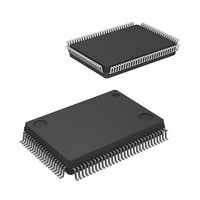
R5F363AENFA#U0 Renesas Electronics America, R5F363AENFA#U0 Datasheet - Page 21

R5F363AENFA#U0
Manufacturer Part Number
R5F363AENFA#U0
Description
MCU 4KB FLASH 256/16K 100-QFP
Manufacturer
Renesas Electronics America
Series
M16C/60/63r
Specifications of R5F363AENFA#U0
Core Processor
M16C/60
Core Size
16/32-Bit
Speed
20MHz
Connectivity
EBI/EMI, I²C, SIO, UART/USART
Peripherals
DMA, LVD, POR, PWM, WDT
Number Of I /o
85
Program Memory Size
256KB (256K x 8)
Program Memory Type
FLASH
Ram Size
20K x 8
Voltage - Supply (vcc/vdd)
1.8 V ~ 5.5 V
Data Converters
A/D 26x10b; D/A 2x8b
Oscillator Type
Internal
Operating Temperature
-20°C ~ 85°C
Package / Case
100-QFP
Lead Free Status / RoHS Status
Lead free / RoHS Compliant
Eeprom Size
-
Available stocks
Company
Part Number
Manufacturer
Quantity
Price
M16C/63 Group
REJ03B0271-0100 Rev.1.00 Sep 15, 2009
Page 19 of 113
Table 1.11
Notes:
Main clock input
Main clock output
Sub clock input
Sub clock output
BCLK output
Clock output
INT interrupt input
NMI interrupt input
Key input interrupt
input
Timer A
Timer B
Three-phase motor
control timer
Real-time clock output
PWM output
Remote control signal
receiver input
Serial interface
UART0 to UART2,
UART5 to UART7
1.
2.
Signal Name
Contact the oscillator manufacturer regarding the oscillation characteristics.
TXD2, SDA2, and SCL2 are N-channel open drain output pins. TXDi, SDAi, and SCLi can be selected as CMOS
output pins or N-channel open drain output pins (i = 0, 1, 5 to 7).
Pin Functions for the 100-Pin Package (2/3)
U, U, V, V, W, W
TB0IN to TB5IN
RXD0 to RXD2,
TA0IN to TA4IN
CTS0 to CTS2,
RTS0 to RTS2,
TXD0 to TXD2,
CLK0 to CLK2,
PWM0, PWM1
IDU, IDV, IDW
PMC0, PMC1
RXD6, RXD7
INT0 to INT2
INT3 to INT7
CTS6, CTS7
RTS6, RTS7
TXD6, TXD7
CLK6, CLK7
TA0OUT to
Pin Name
KI0 to KI7
CLKOUT
TA4OUT
XCOUT
CLKS1
XOUT
TRHO
BCLK
RXD5
CTS5
RTS5
CLK5
TXD5
XCIN
NMI
XIN
SD
ZP
I/O Power Supply
I/O
I/O
I/O
O
O
O
O
O
O
O
O
O
O
O
O
I
I
I
I
I
I
I
I
I
I
I
I
I
I
I
I
VCC1, VCC2 PWM output.
VCC1
VCC1
VCC1
VCC1
VCC2
VCC2
VCC1
VCC2
VCC1
VCC1
VCC1
VCC1
VCC1
VCC1
VCC1
VCC2
VCC1
VCC1
VCC1
VCC2
VCC1
VCC2
VCC1
VCC2
VCC1
VCC2
VCC1
VCC2
VCC1
VCC1
I/O for the main clock oscillator. Connect a ceramic
resonator or crystal between pins XIN and XOUT.
Input an external clock to XIN pin and leave XOUT pin
open.
I/O for a sub clock oscillator. Connect a crystal
between XCIN pin and XCOUT pin.
external clock to XCIN pin and leave XCOUT pin
open.
Outputs the BCLK signal.
Outputs a clock with the same frequency as fC, f1, f8,
or f32.
Input for the INT interrupt.
Input for the NMI interrupt.
Input for the key input interrupt.
I/O for timers A0 to A4 (TA0OUT is N-channel open
drain output).
Input for timers A0 to A4.
Input for Z-phase.
Input for timers B0 to B5.
Output for the three-phase motor control timer.
Forced cutoff input.
Input for the position data.
Output for the real-time clock.
Input for the remote control signal receiver.
Input pins to control data transmission.
Output pins to control data reception.
Transmit/receive clock I/O.
Serial data input.
Serial data output.
Output for the transmit/receive clock multiple-pin output
function.
(2)
Description
(1)
Input an
1. Overview
(1)


