R5F363AENFA#U0 Renesas Electronics America, R5F363AENFA#U0 Datasheet
R5F363AENFA#U0
Specifications of R5F363AENFA#U0
Available stocks


Related parts for R5F363AENFA#U0


R5F363AENFA#U0 Summary of contents
Page 1
To our customers, Old Company Name in Catalogs and Other Documents st On April 1 , 2010, NEC Electronics Corporation merged with Renesas Technology Corporation, and Renesas Electronics Corporation took over all the business of both companies. Therefore, although the ...
Page 2
All information included in this document is current as of the date this document is issued. Such information, however, is subject to change without any prior notice. Before purchasing or using any Renesas Electronics products listed herein, please confirm ...
Page 3
M16C/63 Group 16 HARDWARE MANUAL RENESAS MCU M16C FAMILY / M16C/60 SERIES All information contained in these materials, including products and product specifications, represents information on the product at the time of publication and is subject to change by Renesas ...
Page 4
This document is provided for reference purposes only so that Renesas customers may select the appropriate Renesas products for their use. Renesas neither makes warranties or representations with respect to the accuracy or completeness of the information contained in ...
Page 5
General Precautions in the Handling of MPU/MCU Products The following usage notes are applicable to all MPU/MCU products from Renesas. For detailed usage notes on the products covered by this manual, refer to the relevant sections of the manual. If ...
Page 6
How to Use This Manual 1. Purpose and Target Readers This manual is designed to provide the user with an understanding of the hardware functions and electrical characteristics of the MCU intended for users designing application systems incorporating ...
Page 7
Notation of Numbers and Symbols The notation conventions for register names, bit names, numbers, and symbols used in this manual are described below. (1) Registers, bits, and pins Registers, bits, and pins are indicated by symbols. Each symbol has ...
Page 8
Register Notation The symbols and terms used in register diagrams are described below. • • • Register Bit Symbol *1 Blank box: Set this bit ...
Page 9
List of Abbreviations and Acronyms Abbreviation ACIA Asynchronous Communication Interface Adapter bps bits per second CRC Cyclic Redundancy Check DMA Direct Memory Access DMAC Direct Memory Access Controller GSM Global System for Mobile Communications Hi-Z High Impedance IEBus Inter ...
Page 10
SFR Page Reference .......................................................................................................B-1 1. Overview .................................................................................................. 1 1.1 Features .............................................................................................................. 1 1.1.1 Applications ................................................................................................. 1 1.2 Specifications ...................................................................................................... 2 1.3 Product List ......................................................................................................... 6 1.4 Block Diagram ..................................................................................................... 8 1.5 Pin Assignments................................................................................................ 10 1.6 Pin Functions..................................................................................................... 18 2. Central ...
Page 11
Special Function Registers (SFRs) ........................................................ 29 4.1 SFRs ................................................................................................................. 29 4.2 Notes on SFRs .................................................................................................. 45 4.2.1 Register Settings ....................................................................................... 45 5. Protection ............................................................................................... 46 5.1 Introduction........................................................................................................ 46 5.2 Register ............................................................................................................. 46 5.2.1 Protect Register (PRCR) ........................................................................... 46 5.3 ...
Page 12
Registers ........................................................................................................... 66 7.2.1 Voltage Detector 2 Flag Register (VCR1) .................................................. 67 7.2.2 Voltage Detector Operation Enable Register (VCR2) ................................ 68 7.2.3 Voltage Monitor Function Select Register (VWCE) ................................... 69 7.2.4 Voltage Detector 1 Level Select Register (VD1LS) ................................... ...
Page 13
CPU Clock and Peripheral Function Clocks.................................................... 104 8.4.1 CPU Clock and BCLK .............................................................................. 104 8.4.2 Peripheral Function Clocks (f1, fOCO40M, fOCO-F, fOCO-S, fC32, fC) . 104 8.5 Clock Output Function..................................................................................... 106 8.6 System Clock Protection Function .................................................................. 106 8.7 ...
Page 14
Notes on Power Control .................................................................................. 131 9.6.1 CPU Clock ............................................................................................... 131 9.6.2 Wait Mode ............................................................................................... 131 9.6.3 Stop Mode ............................................................................................... 132 9.6.4 Low Current Consumption Read Mode ................................................... 132 10. Processor Mode ................................................................................... 133 10.1 Introduction...................................................................................................... 133 10.2 Registers ...
Page 15
Registers ......................................................................................................... 162 12.2.1 Data Bank Register (DBR) ...................................................................... 163 12.3 Operations....................................................................................................... 164 12.3.1 1-MB Mode .............................................................................................. 164 12.3.2 4-MB Mode .............................................................................................. 166 13. Programmable I/O Ports....................................................................... 173 13.1 Introduction...................................................................................................... 173 13.2 I/O Ports and Pins ........................................................................................... 174 13.3 ...
Page 16
Interrupt Control Register 2 (INT7IC, INT6IC, INT3IC, S4IC/INT5IC, S3IC/INT4IC, KUPIC, INT0IC to INT2IC) ............ 202 14.2.4 Interrupt Source Select Register 3 (IFSR3A) .......................................... 203 14.2.5 Interrupt Source Select Register 2 (IFSR2A) .......................................... 204 14.2.6 Interrupt Source Select Register (IFSR) ...
Page 17
Address Match Interrupt .................................................................................. 225 14.12 Non-Maskable Interrupt Source Discrimination............................................... 226 14.13 Notes on Interrupts.......................................................................................... 227 14.13.1 Reading Address 00000h ........................................................................ 227 14.13.2 SP Setting ................................................................................................ 227 14.13.3 NMI Interrupt ............................................................................................ 227 14.13.4 Changing an Interrupt Source ................................................................. 228 ...
Page 18
DMA Enabled .......................................................................................... 250 16.3.2 DMA Request .......................................................................................... 250 16.3.3 Transfer Cycles ....................................................................................... 251 16.3.4 DMAC Transfer Cycles ............................................................................ 253 16.3.5 Single Transfer Mode .............................................................................. 254 16.3.6 Repeat Transfer Mode ............................................................................. 255 16.3.7 Channel Priority and DMA Transfer Timing ...
Page 19
One-Shot Timer Mode ............................................................................. 293 17.3.6 Pulse Width Modulation (PWM) Mode ..................................................... 297 17.3.7 Programmable Output Mode (Timers A1, A2, and A4) ............................ 302 17.4 Interrupts ......................................................................................................... 306 17.5 Notes on Timer A ............................................................................................ 307 17.5.1 Common Notes on ...
Page 20
Timer B (Event Counter Mode) ................................................................ 337 18.5.4 Timer B (Pulse Period/Pulse Width Measurement Modes) ..................... 338 19. Three-Phase Motor Control Timer Function ......................................... 339 19.1 Introduction...................................................................................................... 339 19.2 Registers ......................................................................................................... 343 19.2.1 Timer B2 Register (TB2) .......................................................................... 344 ...
Page 21
Day-of-the-Week Data Register (TRHWK) .............................................. 386 20.2.6 Date Data Register (TRHDY) .................................................................. 387 20.2.7 Month Data Register (TRHMON) ............................................................ 388 20.2.8 Year Data Register (TRHYR) ................................................................... 389 20.2.9 Timer RH Control Register (TRHCR) ..................................................... 390 20.2.10 Timer RH Count ...
Page 22
Operation Example .................................................................................. 416 22. Remote Control Signal Receiver .......................................................... 418 22.1 Introduction...................................................................................................... 418 22.2 Registers ......................................................................................................... 421 22.2.1 Peripheral Clock Stop Register (PCLKSTP1) .......................................... 423 22.2.2 PMCi Function Select Register 0 (PMCiCON0 ........................ 424 ...
Page 23
Serial Interface UARTi ( ............................................. 465 23.1 Introduction...................................................................................................... 465 23.2 Registers ......................................................................................................... 470 23.2.1 UART Clock Select Register (UCLKSEL0) .............................................. 472 23.2.2 Peripheral Clock Select Register (PCLKR) ............................................. 472 23.2.3 Peripheral Clock ...
Page 24
Serial Interface SI/O3 and SI/O4.......................................................... 534 24.1 Introduction...................................................................................................... 534 24.2 Registers ......................................................................................................... 536 24.2.1 Peripheral Clock Select Register (PCLKR) ............................................. 537 24.2.2 Peripheral Clock Stop Register (PCLKSTP1) .......................................... 538 24.2.3 SI/Oi Transmit/Receive Register (SiTRR ................................. ...
Page 25
I2C0 Control Register 0 (S1D0) ............................................................... 557 25.2.6 I2C0 Clock Control Register (S20) .......................................................... 560 25.2.7 I2C0 Start/Stop Condition Control Register (S2D0) ................................. 563 25.2.8 I2C0 Control Register 1 (S3D0) ............................................................... 564 25.2.9 I2C0 Control Register 2 (S4D0) ............................................................... ...
Page 26
CEC Receive Buffer Register 2 (CCRB2) ............................................... 613 26.2.11 CEC Receive Follower Address Set Register 1 (CRADRI1), CEC Receive Follower Address Set Register 2 (CRADRI2) ................... 614 26.2.12 Port Control Register (PCR) .................................................................... 615 26.3 Operations....................................................................................................... 616 26.3.1 Standard ...
Page 27
Single Sweep Mode ................................................................................. 654 27.4.4 Repeat Sweep Mode 0 ............................................................................ 656 27.4.5 Repeat Sweep Mode 1 ............................................................................ 658 27.5 External Sensor............................................................................................... 661 27.6 Interrupt ........................................................................................................... 662 27.7 Notes on A/D Converter .................................................................................. 663 27.7.1 Analog Input Pin ...................................................................................... ...
Page 28
Flash Memory....................................................................................... 675 30.1 Introduction...................................................................................................... 675 30.2 Memory Map ................................................................................................... 677 30.3 Registers ......................................................................................................... 679 30.3.1 Flash Memory Control Register 0 (FMR0) ............................................... 679 30.3.2 Flash Memory Control Register 1 (FMR1) ............................................... 682 30.3.3 Flash Memory Control Register 2 ...
Page 29
Electrical Characteristics ...................................................................... 723 31.1 Electrical Characteristics (Common to 1 and 5 V) ............................ 723 31.1.1 Absolute Maximum Rating ....................................................................... 723 31.1.2 Recommended Operating Conditions ..................................................... 724 31.1.3 A/D Conversion Characteristics ............................................................... 729 31.1.4 D/A Conversion ...
Page 30
OSDR Bit (Oscillation Stop Detect Reset Detection Flag) ....................... 793 32.6 Notes on Clock Generator.............................................................................. 794 32.6.1 Oscillation Circuit Using an Oscillator ...................................................... 794 32.6.2 Noise Countermeasure ............................................................................ 795 32.6.3 CPU Clock ............................................................................................... 796 32.6.4 Oscillation Stop/Restart Detect Function ...
Page 31
Common Notes on Multiple Modes ......................................................... 809 32.15.2 Timer A (Timer Mode) .............................................................................. 809 32.15.3 Timer A (Event Counter Mode) ................................................................ 809 32.15.4 Timer A (One-Shot Timer Mode) ............................................................. 810 32.15.5 Timer A (Pulse Width Modulation Mode) ................................................. 811 ...
Page 32
Operation after Reset When Selecting the External Clock ...................... 823 32.23 Notes on Multi-Master I 32.23.1 Limitation on CPU Clock .......................................................................... 824 32.23.2 Register Access ....................................................................................... 824 32.24 Notes on CEC ................................................................................................. 825 32.24.1 Registers and Bit Operation .................................................................... ...
Page 33
SFR Quick Reference Address Register 0000h 0001h 0002h 0003h 0004h Processor Mode Register 0 0005h Processor Mode Register 1 0006h System Clock Control Register 0 0007h System Clock Control Register 1 0008h Chip Select Control Register 0009h External Area Recovery ...
Page 34
Address Register 0079h 007Ah 007Bh I2C-bus Interface Interrupt Control Register 007Ch SCL/SDA Interrupt Control Register 007Dh 007Eh 007Fh 0080h to 017Fh 0180h DMA0 Source Pointer 0181h 0182h 0183h 0184h DMA0 Destination Pointer 0185h 0186h 0187h 0188h DMA0 Transfer Counter 0189h ...
Page 35
Address Register 01FBh PMC1 Function Select Register 3 01FCh PMC1 Status Register 01FDh PMC1 Interrupt Source Select Register 01FEh 01FFh 0200h 0201h 0202h 0203h 0204h 0205h Interrupt Source Select Register 3 0206h Interrupt Source Select Register 2 0207h Interrupt Source ...
Page 36
Address Register 0283h 0284h UART5 Special Mode Register 4 0285h UART5 Special Mode Register 3 0286h UART5 Special Mode Register 2 0287h UART5 Special Mode Register 0288h UART5 Transmit/Receive Mode Register 0289h UART5 Bit Rate Register 028Ah UART5 Transmit Buffer ...
Page 37
Address Register 0346h Year Data Register 0347h Timer RH Control Register 0348h Timer RH Count Source Select Register 0349h Clock Error Correction Register 034Ah Timer RH Interrupt Flag Register 034Bh Timer RH Interrupt Enable Register 034Ch Alarm Minute Register 034Dh ...
Page 38
Address Register 03CAh A/D Register 5 03CBh 03CCh A/D Register 6 03CDh 03CEh A/D Register 7 03CFh 03D0h 03D1h 03D2h 03D3h 03D4h A/D Control Register 2 03D5h 03D6h A/D Control Register 0 03D7h A/D Control Register 1 03D8h D/A0 Register ...
Page 39
M16C/63 Group RENESAS MCU 1. Overview 1.1 Features The M16C/63 Group microcomputer (MCU) incorporates the M16C/60 Series CPU core and flash memory, employing sophisticated instructions for a high level of efficiency. This MCU has address space (expandable ...
Page 40
M16C/63 Group 1.2 Specifications The M16C/63 Group includes 100-pin and 80-pin packages. Table 1.1 to Table 1.4 list specifications. Table 1.1 Specifications for the 100-Pin Package (1/2) Item Function CPU Central processing unit Memory ROM, RAM, data flash Voltage Voltage ...
Page 41
M16C/63 Group Table 1.2 Specifications for the 100-Pin Package (2/2) Item Function Timer A Timer B Three-phase motor control timer functions Timers Real-time clock PWM function Remote control signal receiver UART0 to UART2, UART5 to Serial UART7 Interface SI/O3, SI/O4 ...
Page 42
M16C/63 Group Table 1.3 Specifications for the 80-Pin Package (1/2) Item Function CPU Central processing unit Memory ROM, RAM, data flash Voltage Voltage detector Detection Clock Clock generator External Bus Bus memory expansion Expansion I/O Ports Programmable I/O ports Interrupts ...
Page 43
M16C/63 Group Table 1.4 Specifications for the 80-Pin Package (2/2) Item Function Timer A Timer B Three-phase motor control Timers timer functions Real-time clock PWM function Remote control signal receiver UART0 to UART2, UART5 Serial Interface SI/O3, SI/O4 2 Multi-master ...
Page 44
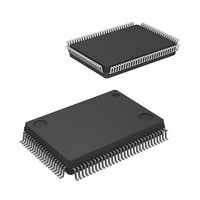
M16C/63 Group 1.3 Product List Table 1.5 lists product information. Figure 1.1 shows the Part No., with Memory Size and Package, and Figure 1.2 and Figure 1.3 shows the Marking Diagram (Top View). Table 1.5 Product List Part No. Program ...
Page 45
M16C/63 Group Part No Figure 1.1 Part No., with Memory Size and Package PRQP0100JD-B (100P6F-A), PLQP0100KB-A (100P6Q-A), PLQP0080KB-A (80P6Q- ...
Page 46
M16C/63 Group 1.4 Block Diagram Figure 1.4 and Figure 1.5 show block diagrams Port P0 Port P1 Internal peripheral functions Timer (16-bit) Outputs (timer A): 5 Inputs (timer B): 6 Three-phase motor control circuit Real-time clock PWM function ...
Page 47
M16C/63 Group 8 Port P0 Internal peripheral functions Timer (16-bit) Outputs (timer A): 5 Inputs (timer B): 6 Real-time clock PWM function (8-bit x 2) Remote control signal receiver (2 circuits) Watchdog timer (15-bit) A/D converter (10-bit resolution x 26 ...
Page 48
M16C/63 Group 1.5 Pin Assignments Figure 1.6 to Figure 1.9 show pin assignments. Table 1.6 to Table 1.9 list pin names. P0_7/AN0_7/ P0_6/AN0_6/D6 83 P0_5/AN0_5/D5 84 P0_4/AN0_4/D4 85 P0_3/AN0_3/D3 P0_2/AN0_2/ P0_1/AN0_1/D1 88 P0_0/AN0_0/D0 89 P10_7/AN7/KI3 90 ...
Page 49
M16C/63 Group 76 P1_2/RXD6/SCL6/D10 77 P1_1/CLK6/D9 78 P1_0/CTS6/RTS6/D8 79 P0_7/AN0_7/D7 80 P0_6/AN0_6/D6 81 P0_5/AN0_5/D5 82 P0_4/AN0_4/D4 83 P0_3/AN0_3/D3 84 P0_2/AN0_2/D2 85 P0_1/AN0_1/D1 P0_0/AN0_0/ P10_7/AN7/KI3 88 P10_6/AN6/KI2 89 P10_5/AN5/KI1 90 P10_4/AN4/KI0 91 P10_3/AN3/KI7 92 P10_2/AN2/KI6 93 P10_1/AN1/KI5 94 AVSS ...
Page 50
M16C/63 Group P4_2 P4_3 J P4_1 P4_0 H P3_6 P3_7 G P3_2 P3_3 F P3_0 VCC2 E P2_6 P2_7 D P2_2 P2_1 C P2_0 P1_7 B P1_4 P1_5 A P1_3 P1_2 10 9 VCC2 ports Notes: 1. ...
Page 51
M16C/63 Group Table 1.6 Pin Names for the 100-Pin Package (1/2) Pin No. Control Pin Port P9_6 2 100 A2 P9_5 P9_4 P9_3 P9_2 6 ...
Page 52
M16C/63 Group Table 1.7 Pin Names for the 100-Pin Package (2/2) Pin No. Control Port Pin P4_3 52 50 K10 P4_2 53 51 J10 P4_1 P4_0 P3_7 56 ...
Page 53
M16C/63 Group 61 P0_6/AN0_6 P0_5/AN0_5 62 P0_4/AN0_4 63 P0_3/AN0_3 64 P0_2/AN0_2 65 P0_1/AN0_1 66 P0_0/AN0_0 67 P10_7/AN7/KI3 68 P10_6/AN6/KI2 69 P10_5/AN5/KI1 70 P10_4/AN4/KI0 71 P10_3/AN3/KI7 72 P10_2/AN2/KI6 73 P10_1/AN1/KI5 74 AVSS 75 P10_0/AN0/KI4 76 VREF 77 AVCC 78 P9_7/ADTRG/SIN4 79 ...
Page 54
M16C/63 Group Table 1.8 Pin Names for the 80-Pin Package (1/2) Pin No. Control Pin Port 1 P9_5 2 P9_4 3 P9_3 4 P9_2 5 P9_0 6 CNVSS 7 XCIN P8_7 8 XCOUT P8_6 RESET 9 10 XOUT 11 VSS ...
Page 55
M16C/63 Group Table 1.9 Pin Names for the 80-Pin Package (2/2) Pin No. Control Pin Port 41 P4_2 42 P4_1 43 P4_0 44 P3_7 45 P3_6 46 P3_5 47 P3_4 48 P3_3 49 P3_2 50 P3_1 51 P3_0 52 P2_7 ...
Page 56
M16C/63 Group 1.6 Pin Functions Table 1.10 Pin Functions for the 100-Pin Package (1/3) Signal Name Pin Name Power supply VCC1, input VCC2, VSS Analog power AVCC, AVSS supply input RESET Reset input CNVSS CNVSS External data bus BYTE width ...
Page 57
M16C/63 Group Table 1.11 Pin Functions for the 100-Pin Package (2/3) Signal Name Pin Name Main clock input XIN Main clock output XOUT Sub clock input XCIN Sub clock output XCOUT BCLK output BCLK Clock output CLKOUT INT0 to INT2 ...
Page 58
M16C/63 Group Table 1.12 Pin Functions for the 100-Pin Package (3/3) Signal Name Pin Name SDA0 to SDA2, UART0 to SDA5 UART2, SDA6, SDA7 UART5 to SCL0 to SCL2, UART7 SCL5 mode SCL6, SCL7 CLK3, CLK4 Serial ...
Page 59
M16C/63 Group Table 1.13 Pin Functions for the 80-Pin Package (1/2) Signal Name Pin Name Power supply VCC1, input VSS Analog power AVCC, supply input AVSS RESET Reset input CNVSS CNVSS Main clock input XIN Main clock output XOUT Sub ...
Page 60
M16C/63 Group Table 1.14 Pin Functions for the 80-Pin Package (2/2) Signal Name Pin Name CTS0, CTS1, CTS5 RTS0, RTS1, RTS5 CLK0, CLK1, Serial interface CLK5 UART0 to UART2, RXD0 to RXD2, UART5 RXD5 TXD0 to TXD2, TXD5 CLKS1 SDA0 ...
Page 61
M16C/63 Group 2. Central Processing Unit (CPU) Figure 2.1 shows the CPU registers. Seven registers (R0, R1, R2, R3, A0, A1, and FB) out of 13 compose a register bank, and there are two register banks. b31 R2 R3 b19 ...
Page 62
M16C/63 Group 2.2 Address Registers (A0 and A1) A0 and A1 are 16-bit registers used for indirect addressing, relative addressing, transfer, arithmetic, and logic operations. A0 can be combined with A1 and used as a 32-bit address register (A1A0). 2.3 ...
Page 63
M16C/63 Group 2.8.8 Stack Pointer Select Flag (U Flag) ISP is selected when the U flag is 0. USP is selected when the U flag is 1. The U flag becomes 0 when a hardware interrupt request is accepted, or ...
Page 64
M16C/63 Group 3. Address Space 3.1 Address Space The M16C/63 Group has address space from 00000h to FFFFFh. Address space is expandable with the memory area expansion function. Addresses 40000h to BFFFFh can be ...
Page 65
M16C/63 Group 3.2 Memory Map Special function registers (SFRs) are allocated from address 00000h to 003FFh and from 0D000h to 0D7FFh. Peripheral function control registers are located here. All blank areas within SFRs are reserved. Do not access these areas. ...
Page 66
M16C/63 Group 3.3 Accessible Area in Each Mode Areas that can be accessed vary depending on processor mode and the status of each control bit. Figure 3.3 shows the Accessible Area in Each Mode. In single-chip mode, the SFRs, internal ...
Page 67
M16C/63 Group 4. Special Function Registers (SFRs) 4.1 SFRs An SFR is a control register for a peripheral function. Table 4.1 to Table 4.15 list SFR information. Table 4.1 SFR Information (1/16) Address 0000h 0001h 0002h 0003h 0004h Processor Mode ...
Page 68
M16C/63 Group Table 4.2 SFR Information (2/16) Address 0020h 0021h 0022h 40 MHz On-Chip Oscillator Control Register 0 0023h 0024h 0025h 0026h Voltage Monitor Function Select Register 0027h 0028h Voltage Detector 1 Level Select Register 0029h 002Ah Voltage Monitor 0 ...
Page 69
M16C/63 Group Table 4.3 SFR Information (3/16) Address 0050h UART2 Receive Interrupt Control Register 0051h UART0 Transmit Interrupt Control Register 0052h UART0 Receive Interrupt Control Register 0053h UART1 Transmit Interrupt Control Register 0054h UART1 Receive Interrupt Control Register 0055h Timer ...
Page 70
M16C/63 Group Table 4.4 SFR Information (4/16) Address 0180h DMA0 Source Pointer 0181h 0182h 0183h 0184h DMA0 Destination Pointer 0185h 0186h 0187h 0188h DMA0 Transfer Counter 0189h 018Ah 018Bh 018Ch DMA0 Control Register 018Dh 018Eh 018Fh 0190h DMA1 Source Pointer ...
Page 71
M16C/63 Group Table 4.5 SFR Information (5/16) Address 01B0h DMA3 Source Pointer 01B1h 01B2h 01B3h 01B4h DMA3 Destination Pointer 01B5h 01B6h 01B7h 01B8h DMA3 Transfer Counter 01B9h 01BAh 01BBh 01BCh DMA3 Control Register 01BDh 01BEh 01BFh 01C0h Timer B0-1 Register ...
Page 72
M16C/63 Group Table 4.6 SFR Information (6/16) Address 01E0h Timer B3-1 Register 01E1h 01E2h Timer B4-1 Register 01E3h 01E4h Timer B5-1 Register 01E5h 01E6h Pulse Period/Pulse Width Measurement Mode Function Select Register 2 01E7h 01E8h Timer B Count Source Select ...
Page 73
M16C/63 Group Table 4.7 SFR Information (7/16) Address 0210h Address Match Interrupt Register 0 0211h 0212h 0213h 0214h Address Match Interrupt Register 1 0215h 0216h 0217h 0218h Address Match Interrupt Register 2 0219h 021Ah 021Bh 021Ch Address Match Interrupt Register ...
Page 74
M16C/63 Group Table 4.8 SFR Information (8/16) Address 0240h 0241h 0242h 0243h 0244h UART0 Special Mode Register 4 0245h UART0 Special Mode Register 3 0246h UART0 Special Mode Register 2 0247h UART0 Special Mode Register 0248h UART0 Transmit/Receive Mode Register ...
Page 75
M16C/63 Group Table 4.9 SFR Information (9/16) Address 0270h SI/O3 Transmit/Receive Register 0271h 0272h SI/O3 Control Register 0273h SI/O3 Bit Rate Register 0274h SI/O4 Transmit/Receive Register 0275h 0276h SI/O4 Control Register 0277h SI/O4 Bit Rate Register 0278h SI/O3, 4 Control ...
Page 76
M16C/63 Group Table 4.10 SFR Information (10/16) Address 02A0h 02A1h 02A2h 02A3h 02A4h UART7 Special Mode Register 4 02A5h UART7 Special Mode Register 3 02A6h UART7 Special Mode Register 2 02A7h UART7 Special Mode Register 02A8h UART7 Transmit/Receive Mode Register ...
Page 77
M16C/63 Group Table 4.11 SFR Information (11/16) Address 0310h Timer B3 Register 0311h 0312h Timer B4 Register 0313h 0314h Timer B5 Register 0315h 0316h 0317h 0318h Port Function Control Register 0319h 031Ah 031Bh Timer B3 Mode Register 031Ch Timer B4 ...
Page 78
M16C/63 Group Table 4.12 SFR Information (12/16) Address 0340h Second Data Register 0341h Minute Data Register 0342h Hour Data Register 0343h Day-of-the-Week Data Register 0344h Date Data Register 0345h Month Data Register 0346h Year Data Register 0347h Timer RH Control ...
Page 79
M16C/63 Group Table 4.13 SFR Information (13/16) Address 0370h PWM Control Register 0 0371h 0372h PWM0 Prescaler 0373h PWM0 Register 0374h PWM1 Prescaler 0375h PWM1 Register 0376h PWM Control Register 1 0377h 0378h 0379h 037Ah 037Bh 037Ch Count Source Protection ...
Page 80
M16C/63 Group Table 4.14 SFR Information (14/16) Address 03A0h 03A1h 03A2h Open-Circuit Detection Assist Function Register 03A3h 03A4h 03A5h 03A6h 03A7h 03A8h 03A9h 03AAh 03ABh 03ACh 03ADh 03AEh 03AFh 03B0h 03B1h 03B2h 03B3h 03B4h SFR Snoop Address Register 03B5h 03B6h ...
Page 81
M16C/63 Group Table 4.15 SFR Information (15/16) Address 03D0h 03D1h 03D2h 03D3h 03D4h A/D Control Register 2 03D5h 03D6h A/D Control Register 0 03D7h A/D Control Register 1 03D8h D/A0 Register 03D9h 03DAh D/A1 Register 03DBh 03DCh D/A Control Register ...
Page 82
M16C/63 Group Table 4.16 SFR Information (16/16) Address D080h PMC0 Header Pattern Set Register (Min) D081h D082h PMC0 Header Pattern Set Register (Max) D083h D084h PMC0 Data 0 Pattern Set Register (Min) D085h PMC0 Data 0 Pattern Set Register (Max) ...
Page 83
M16C/63 Group 4.2 Notes on SFRs 4.2.1 Register Settings Table 4.17 lists Registers with Write-Only Bits and registers whose function differs between reading and writing. Set these registers with immediate values. When establishing the next value by altering the existing ...
Page 84
M16C/63 Group 5. Protection 5.1 Introduction In the event that a program runs out of control, this function protects the important registers listed below so that they will not be rewritten easily. 5.2 Register Table 5.1 Registers Address 000Ah Protect ...
Page 85
M16C/63 Group PRC6, PRC3, PRC1, PRC0 (Protect bits (b6, b3, b1, b0) When setting bits PRC6, PRC3, PRC1, and PRC0 to 1 (write enabled), the bits remain 1 (write enabled). To change registers protected by these ...
Page 86
M16C/63 Group 5.3 Notes on Protection After setting the PRC2 bit to 1 (write enabled), by writing to a given SFR, the PRC2 bit becomes 0 (write disabled). Change the registers protected by the PRC2 bit in the next instruction ...
Page 87
M16C/63 Group 6. Resets 6.1 Introduction The following resets can be used to reset the MCU: hardware reset, power-on reset, voltage monitor 0 reset, voltage monitor 1 reset, voltage monitor 2 reset, oscillator stop detect reset, watchdog timer reset, and ...
Page 88
M16C/63 Group Table 6.2 I/O Pins Pin I/O RESET Input VCC1 Input XIN Input 6.2 Registers Refer to 7. “Voltage Detector” for registers used with the voltage monitor 0 reset, voltage monitor 1 reset, and voltage monitor 2 reset. Refer ...
Page 89
M16C/63 Group 6.2.1 Processor Mode Register 0 (PM0) Processor Mode Register Symbol PM0 Bit Symbol PM00 PM01 PM02 PM03 PM04 PM05 PM06 PM07 Write to this register after setting the PRC1 ...
Page 90
M16C/63 Group 6.2.2 Reset Source Determine Register (RSTFR) Reset Source Determine Register Symbol RSTFR Bit Symbol CWR HWR SWR WDR LVD1R LVD2R OSDR — (b7) Table 6.4 RSTFR Register Reset Value ...
Page 91
M16C/63 Group 6.3 Optional Function Select Area In the optional function select area, the MCU state after reset and the function to prevent rewrite in parallel I/O mode are selected. The optional function select area is not an SFR, and ...
Page 92
M16C/63 Group ROMCR (ROM code protect cancel bit) (b2) ROMCP1 (ROM code protect bit) (b3) These bits prevent the flash memory from being read or changed in parallel I/O mode. Table 6.5 ROM Code Protection Bit Setting ROMCR bit 0 ...
Page 93
M16C/63 Group 6.4 Operations 6.4.1 Status after Reset The status of SFRs after reset depends on the reset type. See the Reset Value column in 4. “Special Function Registers (SFRs)”. Table 6.6 lists the Pin Status When RESET Pin Level ...
Page 94
M16C/63 Group b15 b19 Content of addresses FFFFEh to FFFFCh b15 b15 b15 IPL Figure 6.2 CPU Register Status after Reset REJ09B0510-0100 Rev.1.00 Sep 15, 2009 Page 56 of 836 b0 0000h 0000h 0000h 0000h 0000h 0000h 0000h b0 00000h ...
Page 95
M16C/63 Group VCC1, VCC2 XIN td(P-R) Microprocessor mode BYTE = high RESET BCLK Address RD WR CS0 Microprocessor mode BYTE = low Address RD WR CS0 Single-chip mode Address Figure 6.3 Reset Sequence REJ09B0510-0100 Rev.1.00 Sep 15, 2009 Page 57 ...
Page 96
M16C/63 Group 6.4.2 Hardware Reset This reset is triggered by the RESET pin. When the power supply voltage meets the recommended operating conditions, the MCU resets the pins, CPU, and SFRs when a low-level signal is applied to the RESET ...
Page 97
M16C/63 Group 6.4.3 Power-On Reset Function The power-on reset function can be used on the system in which VCC1 is Vdet0 or higher. When the RESET pin is connected to VCC1 via a pull-up resistor, and the VCC1 voltage level ...
Page 98
M16C/63 Group 6.4.4 Voltage Monitor 0 Reset This reset is triggered by the MCU's on-chip voltage detector 0. The voltage detector 0 monitors the voltage applied to the VCC1 pin (Vdet0). The MCU resets the pins, CPU, and SFRs when ...
Page 99
M16C/63 Group 6.4.7 Oscillator Stop Detect Reset The MCU resets and stops the pins, CPU, and SFRs when the CM27 bit in the CM2 register is 0 (reset when oscillator stop detected detects that the main clock oscillator ...
Page 100
M16C/63 Group 6.4.10 Cold/Warm Start Discrimination The cold/warm start discrimination detects whether or not voltage applied to the VCC1 pin drops to the RAM hold voltage or below. The reference voltage is Vdet0. Therefore, the voltage monitor 0 reset is ...
Page 101
M16C/63 Group 6.5 Notes on Resets 6.5.1 Power Supply Rising Gradient When supplying power to the MCU, make sure that the power supply voltage applied to the VCC1 pin meets the SVCC conditions. Symbol Power supply V CC1 (Voltage range: ...
Page 102
M16C/63 Group 7. Voltage Detector 7.1 Introduction The voltage detector monitors the voltage applied to the VCC1 pin. This circuit can be programmed to monitor the VCC1 input voltage. Voltage monitor 0 reset, voltage monitor 1 interrupt, voltage monitor 1 ...
Page 103
M16C/63 Group VCC1 Internal reference voltage Figure 7.1 Voltage Detector Block Diagram REJ09B0510-0100 Rev.1.00 Sep 15, 2009 Page 65 of 836 VC27 + ≥ Vdet2 - VC26 + ≥ Vdet1 - VC25 + - ≥ Vdet0 VCR27, VCR26, VCR25: Bits ...
Page 104
M16C/63 Group 7.2 Registers Table 7.2 Registers Address 0019h Voltage Detector 2 Flag Register 001Ah Voltage Detector Operation Enable Register 0026h Voltage Monitor Function Select Register 0028h Voltage Detector 1 Level Select Register 002Ah Voltage Monitor 0 Control Register 002Bh ...
Page 105
M16C/63 Group 7.2.1 Voltage Detector 2 Flag Register (VCR1) Voltage Detector 2 Flag Register Symbol VCR1 Bit Symbol — (b2-b0) VC13 — (b7-b4) This register ...
Page 106
M16C/63 Group 7.2.2 Voltage Detector Operation Enable Register (VCR2) Voltage Detector Operation Enable Register Symbol VCR2 Bit Symbol — (b3-b0) — (b4) VC25 VC26 VC27 Notes: 1. This ...
Page 107
M16C/63 Group 7.2.3 Voltage Monitor Function Select Register (VWCE) Voltage Monitor Function Select Register Symbol VWCE Bit Symbol VW12E — (b7-b1) Set the PRC3 bit ...
Page 108
M16C/63 Group 7.2.4 Voltage Detector 1 Level Select Register (VD1LS) Voltage Detector 1 Level Select Register Symbol VD1LS Bit Symbol VD1LS0 VD1LS1 VD1LS2 VD1LS3 — (b7-b4) Set the ...
Page 109
M16C/63 Group 7.2.5 Voltage Monitor 0 Control Register (VW0C) Voltage Monitor 0 Control Register Symbol VW0C Bit Symbol VW0C0 VW0C1 — (b2) — (b3) VW0F0 VW0F1 — (b7-b6) Notes: ...
Page 110
M16C/63 Group 7.2.6 Voltage Monitor 1 Control Register (VW1C) Voltage Monitor 1 Control Register Symbol VW1C Bit Symbol VW1C0 VW1C1 VW1C2 VW1C3 VW1F0 VW1F1 VW1C6 VW1C7 Set the PRC3 bit in the ...
Page 111
M16C/63 Group VW1C2 (Voltage change detection flag) (b2) The VW1C2 bit is enabled when the VC26 bit in the VCR2 register is 1 (voltage detector 1 enabled). This bit does not change even if set to 1. Condition to become ...
Page 112
M16C/63 Group 7.2.7 Voltage Monitor 2 Control Register (VW2C) Voltage Monitor 2 Control Register Symbol VW2C Bit Symbol VW2C0 VW2C1 VW2C2 VW2C3 VW2F0 VW2F1 VW2C6 VW2C7 Set the PRC3 bit in the ...
Page 113
M16C/63 Group VW2C2 (Voltage change detection flag) (b2) The VW2C2 bit is enabled when the VC27 bit in the VCR2 register is 1 (voltage detector 2 enabled). This bit does not change even if set to 1. Condition to become ...
Page 114
M16C/63 Group 7.3 Optional Function Select Area In the optional function select area, the MCU state after reset and the function to prevent rewrite in parallel I/O mode are selected. The optional function select area is not an SFR, and ...
Page 115
M16C/63 Group 7.4 Operations 7.4.1 Digital Filter A digital filter can be used to monitor VCC1 input voltage. For the voltage detector 2), the digital filter is enabled when the VWiC1 bit in the VWiC ...
Page 116
M16C/63 Group 7.4.2 Voltage Detector 0 When the VC25 bit in the VCR2 register is 1 (voltage detector 0 enabled), voltage detector 0 monitors the voltage applied to the VCC1 pin and detects whether the voltage rises through or falls ...
Page 117
M16C/63 Group 7.4.2.1 Voltage Monitor 0 Reset When using voltage monitor 0 reset, set the VDSEL1 bit in the OFS1 address to 0 (Vdet0 is 2.85 V (Vdet0_2)). Table 7.6 lists Procedures for Setting Voltage Monitor 0 Reset Related Bits. ...
Page 118
M16C/63 Group 7.4.3 Voltage Detector 1 When the VW12E bit in the VWCE register is 1 (voltage detectors 1 and 2 enabled) and the VC26 bit in the VCR2 register is 1 (voltage detector 1 enabled), voltage detector 1 monitors ...
Page 119
M16C/63 Group 7.4.3.2 Voltage Monitor 1 Interrupt and Voltage Monitor 1 Reset Table 7.7 lists Procedures for Setting Voltage Monitor 1 Interrupt/Reset Related Bits. Table 7.7 Procedures for Setting Voltage Monitor 1 Interrupt/Reset Related Bits When Using the Digital Filter ...
Page 120
M16C/63 Group Vdet1 VW1C3 bit VW1C2 bit When the VW1C1 bit is 0 (digital filter Voltage monitor 1 enabled) interrupt request (when VW1C6 is 0) Internal reset signal (when VW1C6 is 1) When the VW1C1 bit is 1 (digital filter ...
Page 121
M16C/63 Group 7.4.4 Voltage Detector 2 When the VW12E bit in the VWCE register is 1 (voltage detectors 1 and 2 enabled) and the VC27 bit in the VCR2 register is 1 (voltage detector 2 enabled), the voltage detector 2 ...
Page 122
M16C/63 Group 7.4.4.2 Voltage Monitor 2 Interrupt and Voltage Monitor 2 Reset Table 7.8 lists Steps to Set Voltage Monitor 2 Interrupt/Reset Related Bits. Table 7.8 Steps to Set Voltage Monitor 2 Interrupt/Reset Related Bits When Using the Digital Filter ...
Page 123
M16C/63 Group Vdet2 VC13 bit VW2C2 bit When the VW2C1 bit is 0 (digital filter Voltage monitor 2 enabled) interrupt request (when VW2C6 is 0) Internal reset signal (when VW2C6 is 1) When the VW2C1 bit is VW2C2 bit 1 ...
Page 124
M16C/63 Group 7.5 Interrupts The voltage monitor 1 interrupt and voltage monitor 2 interrupt are non-maskable interrupts. The watchdog timer interrupt, oscillator stop/restart detect interrupt, voltage monitor 1 interrupt, and voltage monitor 2 interrupt share the same vector. When using ...
Page 125
M16C/63 Group 8. Clock Generator 8.1 Introduction The clock generator generates operating clocks for the CPU and peripheral functions. Four circuits are incorporated to generate the system clock signals. • Main clock oscillation circuit • 40 MHz on-chip oscillator • ...
Page 126
M16C/63 Group Sub clock oscillation circuit XCIN XCOUT CM04 CM03 40 MHz FRA00 on-chip oscillator 125 kHz CM14 on-chip oscillator CM10 = (stop mode) XIN XOUT R Main clock oscillation circuit CM05 S Q WAIT R instruction ...
Page 127
M16C/63 Group Table 8.2 I/O Pins Pin Name I/O XIN Input XOUT Output XCIN Input XCOUT Output CLKOUT Output BCLK Output Note: 1. Set the port direction bits which share pins to 0 (input mode). 8.2 Registers Table 8.3 Registers ...
Page 128
M16C/63 Group 8.2.1 Processor Mode Register 0 (PM0) Processor Mode Register Symbol PM0 Bit Symbol PM00 PM01 PM02 PM03 PM04 PM05 PM06 PM07 Set the PRC1 bit in the PRCR register ...
Page 129
M16C/63 Group 8.2.2 System Clock Control Register 0 (CM0) System Clock Control Register Symbol CM0 Bit Symbol CM00 CM01 CM02 CM03 CM04 CM05 CM06 CM07 Set the PRC0 bit in the ...
Page 130
M16C/63 Group CM02 (Wait mode peripheral function clock stop bit) (b2) This bit is used to stop the f1 peripheral function clock in wait mode. The fC, fC32, fOCO-S, fOCO-F, and fOCO40M are not affected by the CM02 bit. When ...
Page 131
M16C/63 Group 8.2.3 System Clock Control Register 1 (CM1) System Clock Control Register Symbol 0 0 CM1 Bit Symbol CM10 — (b2-b1) CM13 CM14 CM15 CM16 CM17 Rewrite the CM1 register ...
Page 132
M16C/63 Group CM13 (XIN-XOUT feedback resistor select bit) (b3) The CM13 bit can be used when the main clock is not used at all, or when the externally generated clock is supplied to the XIN pin. When connecting a ceramic ...
Page 133
M16C/63 Group 8.2.4 Oscillation Stop Detection Register (CM2) Oscillation Stop Detection Register Symbol 0 0 CM2 Bit Symbol CM20 CM21 CM22 CM23 — (b5-b4) — (b6) CM27 Rewrite the CM2 register after ...
Page 134
M16C/63 Group CM22 (Oscillator stop/restart detect flag) (b2) Condition to become 0: • Set Conditions to become 1: • Main clock stop is detected. • Main clock restart is detected. (The CM22 bit remains unchanged even if ...
Page 135
M16C/63 Group 8.2.5 Peripheral Clock Select Register (PCLKR) Peripheral Clock Select Register Symbol PCLKR Bit Symbol PCLK0 PCLK1 — (b4-b2) PCLK5 — (b7-b6) Write to the PCLKR ...
Page 136
M16C/63 Group 8.2.7 Peripheral Clock Stop Register (PCLKSTP1) Peripheral Clock Stop Register Set the PRC0 bit in the PRCR register to 1 (write enabled) before rewriting this register REJ09B0510-0100 Rev.1.00 Sep ...
Page 137
M16C/63 Group 8.2.8 Processor Mode Register 2 (PM2) Processor Mode Register Symbol 0 1 PM2 Bit Symbol — (b0) PM21 — (b2) — (b3) PM24 PM25 — (b7-b6) Set the PRC1 ...
Page 138
M16C/63 Group 8.2.9 40 MHz On-Chip Oscillator Control Register 0 (FRA0) 40 MHz On-Chip Oscillator Control Register Symbol FRA0 Bit Symbol FRA00 FRA01 — (b7-b2) Rewrite the FRA0 register after setting ...
Page 139
M16C/63 Group 8.3 Clocks Generated by Clock Generators Clocks generated by the clock generators are described below. 8.3.1 Main Clock This clock is supplied by the main clock oscillator circuit and used as a clock source for the CPU and ...
Page 140
M16C/63 Group 8.3.2 fOCO40M fOCO40M MHz clock (approx.) supplied by the 40 MHz on-chip oscillator the clock source for φ the A/D converter. Follow the steps below to start or stop the 40 ...
Page 141
M16C/63 Group 8.3.5 Sub Clock (fC) The sub clock is supplied by the sub clock oscillator circuit. This clock is the clock source for count sources of the CPU clock, timer A, timer B, real-time clock, CEC function, and remote ...
Page 142
M16C/63 Group 8.4 CPU Clock and Peripheral Function Clocks The CPU is run by the CPU clock, and the peripheral functions are run by the peripheral function clocks. 8.4.1 CPU Clock and BCLK The CPU clock is an operating clock ...
Page 143
M16C/63 Group CPU clock Clock generator Divider Main clock Divider fOCO40M 125 kHz on-chip oscillator clock Divider 1/32 Sub clock PM25 PM25: Bit in the PM2 register PCKSTP16 to PCKSTP10: Bits in the PCLKSTP1 register Figure 8.4 Peripheral Function Clocks ...
Page 144
M16C/63 Group 8.5 Clock Output Function In single-chip mode, the f1, f8, f32 or fC clock can be output from the CLKOUT pin. Use bits CM01 to CM00 in the CM0 register, and the PCLK5 bit in the PCLKR register ...
Page 145
M16C/63 Group 8.7 Oscillator Stop/Restart Detect Function This function detects a stop/restart of the main clock oscillation circuit. The oscillator stop/restart detect function can be enabled and disabled with the CM20 bit in the CM2 register. A reset or oscillator ...
Page 146
M16C/63 Group 8.7.2 Operation When CM27 Bit is 1 (Oscillator Stop/Restart Detect Interrupt) When the CM20 bit is 1 (oscillator stop/restart detect function enabled), the system is placed in the state shown in Table 8.6 if the main clock detects ...
Page 147
M16C/63 Group 8.7.3 Using the Oscillator Stop/Restart Detect Function After oscillator stop is detected, if the main clock re-oscillates, set the main clock back to the clock source for the CPU clock and peripheral functions by a program. Figure 8.5 ...
Page 148
M16C/63 Group 8.9 Notes on Clock Generator 8.9.1 Oscillation Circuit Using an Oscillator The following items should be observed when connecting an oscillator: • The oscillation characteristics are tied closely to the user’s board design. Perform a careful evaluation of ...
Page 149
M16C/63 Group 8.9.2 Noise Countermeasure 8.9.2.1 Clock I/O Pin Wiring • Connect the shortest possible wiring to the clock I/O pin. • Connect (a) the capacitor's ground lead connected to the oscillator, and (b) the MCU's VSS pin, with the ...
Page 150
M16C/63 Group 8.9.2.3 Signal Line Whose Level Changes at a High-Speed For a signal line whose level changes at a high-speed, wire it as far away from the oscillator and the oscillator wiring pattern as possible. Do not wire it ...
Page 151
M16C/63 Group 9. Power Control 9.1 Introduction This chapter describes how to reduce the amount of current consumption. 9.2 Registers Refer to 8. “Clock Generator” for the clock-related registers. Table 9.1 Registers Address Register 0220h Flash Memory Control Register 0 ...
Page 152
M16C/63 Group 9.2.1 Flash Memory Control Register 0 (FMR0) Flash Memory Control Register Symbol 0 0 FMR0 Bit Symbol FMR00 FMR01 FMR02 FMSTP — (b4) — (b5) FMR06 FMR07 FMR01 (CPU ...
Page 153
M16C/63 Group 9.2.2 Flash Memory Control Register 2 (FMR2) Flash Memory Control Register Symbol 0 0 Bit Symbol — (b1-b0) FMR22 FMR23 — (b7-b4) FMR22 (Slow read mode enable bit) (b2) ...
Page 154
M16C/63 Group 9.3 Clock The amount of current consumption correlates with the number of operating clocks and frequency. If there are fewer operating clocks and a lower frequency, current consumption will be low. Normal operating mode, wait mode, and stop ...
Page 155
M16C/63 Group 9.3.1.3 125 kHz On-Chip Oscillator Mode The fOCO-S clock divided by 1 (no division used as the CPU clock. f1 with the same frequency of the fOCO-S clock divided ...
Page 156
M16C/63 Group Table 9.2 Clocks in Normal Operating Mode Mode CPU Clock Main clock High-speed mode divided by 1 Main clock Medium-speed mode divided MHz on- fOCO-F chip oscillator divided by n mode 125 kHz on- fOCO-S ...
Page 157
M16C/63 Group Table 9.3 Clock-Related Bit Setting and Modes CM2 Register CM1 Register Mode High-speed mode, medium-speed mode 40 MHz on-chip oscillator mode 125 kHz on-chip oscillator mode 125 kHz on-chip oscillator low power mode Low-speed mode Low power mode ...
Page 158
M16C/63 Group 9.3.2 Clock Mode Transition Procedure Figure 9.1 shows Clock Mode Transition. Arrows indicate possible mode transitions. Normal Operating Mode 40 MHz on-chip oscillator mode d a High-speed or medium-speed mode Interrupt or reset CPU operation stop Figure 9.1 ...
Page 159
M16C/63 Group a. Entering high-speed mode or medium-speed mode from 40 MHz on-chip oscillator mode, 125 kHz on-chip oscillator mode, or low-speed mode (1) Select the main clock and wait until the oscillation stabilizes. Refer to 8.3.1 “Main Clock”. (2) ...
Page 160
M16C/63 Group 9.3.3 Wait Mode In wait mode, the CPU clock, CPU, watchdog timer, and NMI / SD digital filter are turned off as they are operated by the CPU clock. However, if the CSPRO bit in the CSPR register ...
Page 161
M16C/63 Group Table 9.8 Resets and Interrupts to Exit Wait Mode and Conditions for Use Interrupt, Reset INT Key input Timer A, timer B Remote control signal receiver Peripheral function Serial interrupt interface Interrupt Multi-master 2 I C-bus interface CEC ...
Page 162
M16C/63 Group When the MCU exits wait mode by hardware reset, voltage monitor 0 reset, voltage monitor 1 reset, voltage monitor 2 reset, watchdog timer reset, NMI interrupt, voltage monitor 1 interrupt, or voltage monitor 2 interrupt, set bits ILVL2 ...
Page 163
M16C/63 Group 9.3.4 Stop Mode In stop mode, all oscillator circuits, the CPU clock, and peripheral function clocks are stopped. Therefore, the CPU and the peripheral functions using these clocks stop operating. The least amount of power is consumed in ...
Page 164
M16C/63 Group 9.3.4.3 Exiting Stop Mode Use a reset or an interrupt to exit stop mode. Table 9.10 lists Resets and Interrupts to Exit Stop Mode and Conditions for Use. Table 9.10 Resets and Interrupts to Exit Stop Mode and ...
Page 165
M16C/63 Group 9.4 Power Control in Flash Memory 9.4.1 Stopping Flash Memory When the flash memory is stopped, current consumption is reduced. Execute a program in any area other than the flash memory. Figure 9.2 shows Stop and Restart of ...
Page 166
M16C/63 Group 9.4.2 Reading Flash Memory Current consumption while reading the flash memory can be reduced by using bits FMR22 and FMR23. 9.4.2.1 Slow Read Mode Slow read mode can be used when f(BCLK) is below or equal to f(SLOW_R). ...
Page 167
M16C/63 Group 9.4.2.2 Low Current Consumption Read Mode Low current consumption read mode can be used when the CM07 bit in the CM0 register is 1 (sub clock used as CPU clock). Figure 9.4 shows Setting and Canceling Low Current ...
Page 168
M16C/63 Group 9.5 Reducing Power Consumption To reduce power consumption, refer to the following descriptions when designing a system or writing a program. 9.5.1 Ports The MCU retains the state of each I/O port even when it enters wait mode ...
Page 169
M16C/63 Group 9.6 Notes on Power Control 9.6.1 CPU Clock When switching the CPU clock's clock source, wait until oscillation of the switch destination is stable before switching sources. 9.6.2 Wait Mode • Insert four or more NOP instructions following ...
Page 170
M16C/63 Group 9.6.3 Stop Mode When exiting stop mode by hardware reset, drive the RESET pin low until main clock oscillation is • stabilized. • Set the MR0 bit in the TAiMR register ( ...
Page 171
M16C/63 Group 10. Processor Mode Note Do not use memory expansion mode and microprocessor mode in the 80-pin package. Also when VCC2 < 2 not use memory expansion mode and microprocessor mode. 10.1 Introduction Single-chip mode, memory expansion ...
Page 172
M16C/63 Group 10.2 Registers Table 10.3 Registers Address Register 0004h Processor Mode Register 0 0005h Processor Mode Register 1 0010h Program 2 Area Control Register 10.2.1 Processor Mode Register 0 (PM0) Processor Mode Register ...
Page 173
M16C/63 Group 10.2.2 Processor Mode Register 1 (PM1) Processor Mode Register Symbol PM1 Bit Symbol PM10 PM11 PM12 PM13 PM14 PM15 — (b6) PM17 Rewrite this register after setting the ...
Page 174
M16C/63 Group PM13 (Internal area expansion bit 0) (b3) This bit is used to select the range of the RAM, program ROM 1, and external area. When the PM13 bit is 0, the size of the RAM and program ROM ...
Page 175
M16C/63 Group 10.2.3 Program 2 Area Control Register (PRG2C) Program 2 Area Control Register Symbol PRG2C Bit Symbol PRG2C0 (b1) — (b7-b2) Rewrite this register after setting the PRC6 bit in the ...
Page 176
M16C/63 Group 10.3 Operations 10.3.1 Processor Mode Settings Processor mode is set by using the CNVSS pin and bits PM01 to PM00 in the PM0 register. In hardware reset, power-on reset, or voltage monitor 0 reset, the processor mode is ...
Page 177
M16C/63 Group Figure 10.1 shows Memory Map in Single-Chip Mode. Single-Chip Mode 00000h SFR 00400h Internal RAM XXXXXh Reserved area 0D000h SFR 0D800h Reserved area 0E000h (2) Internal ROM (data flash) 10000h (3) Internal ROM (program ROM 2) 14000h Reserved ...
Page 178
M16C/63 Group 11. Bus Note Do not use bus control pins for the 80-pin package. Also when VCC2 < 2 not use bus control pins. 11.1 Introduction Two types of buses are available: • Internal bus in the ...
Page 179
M16C/63 Group 11.2.1 Chip Select Control Register (CSR) Chip Select Control Register Symbol CSR Bit Symbol CS0 CS1 CS2 CS3 CS0W CS1W CS2W CS3W CSiW (CSi wait bit ...
Page 180
M16C/63 Group 11.2.2 Chip Select Expansion Control Register (CSE) Chip Select Expansion Control Register Symbol Bit Symbol CSE00W CSE01W CSE10W CSE11W CSE20W CSE21W CSE30W CSE31W Set the CSiW bit ( ...
Page 181
M16C/63 Group 11.2.3 External Area Wait Control Expansion Register (EWC) External Area Wait Control Expansion Register Symbol EWC Bit Symbol EWC00 EWC01 EWC10 EWC11 EWC20 EWC21 EWC30 EWC31 This register can be ...
Page 182
M16C/63 Group 11.2.4 External Area Recovery Cycle Control Register (EWR) External Area Recovery Cycle Control Register Symbol EWR Bit Symbol EWR0 EWR1 — (b7-b2) The EWR register is enabled when bits CSEi1W ...
Page 183
M16C/63 Group 11.3 Operations 11.3.1 Common Specifications between the Internal Bus and External Bus 11.3.1.1 Reference Clock Both the internal and external buses operate based on the BCLK. However, the area accessed and wait states affect bus operation. Refer to ...
Page 184
M16C/63 Group 11.3.2 Internal Bus The internal bus is used to access the internal area in the MCU. 11.3.2.1 Software Wait States of the Internal Bus The PM17 bit in the PM1 register, which is a software-wait-related bit, affects both ...
Page 185
M16C/63 Group 11.3.3 External Bus The external bus is used to access external devices in memory expansion mode or microprocessor mode. In memory expansion or microprocessor mode, some pins serve as the bus control pins to perform data input to ...
Page 186
M16C/63 Group 11.3.5 External Bus Control The following describes the signals needed for accessing external devices and the functionality of software wait states. 11.3.5.1 Address Bus The address bus consists of 20 lines A19. The address bus width ...
Page 187
M16C/63 Group Example 1 Accessing the external area indicated by CSj in the next cycle after accessing the external area indicated by CSi. The address bus and chip select signal both change state between these two cycles. Access to the ...
Page 188
M16C/63 Group 11.3.5.4 Read and Write Signals When the data bus is 16 bits wide, the read and write signals can be selected based on combinations BHE , and combinations WRL ...
Page 189
M16C/63 Group RDY Signal 11.3.5.6 This signal is provided for accessing external devices which need to be accessed at low speed. If input to the RDY pin is low at the last falling edge of BCLK in the bus cycle, ...
Page 190
M16C/63 Group HOLD Signal 11.3.5.7 This signal is used to transfer control of the bus from the CPU or DMAC to an external circuit. When input to the HOLD pin is pulled low, the bus is placed in a hold ...
Page 191
M16C/63 Group Table 11.9 Pin Functions for Each Processor Mode Processor Mode Bits PM05 to PM04 00b (separate bus) Data bus width 8 bits BYTE Pin High P0_0 to P0_7 P1_0 to P1_7 I/O ports P2_0 A0 ...
Page 192
M16C/63 Group 11.3.5.9 External Bus Status When Internal Area is Accessed Table 11.10 lists the External Bus Status When an Internal Area is Accessed. Figure 11.5 shows the Typical Bus Timings When Accessing SFRs. Table 11.10 External Bus Status When ...
Page 193
M16C/63 Group 11.3.5.10 Software Wait States The PM17 bit in the PM1 register, which is a software-wait-related bit, affects both the internal memory and the external area. Software wait states can be inserted to the external area by setting the ...
Page 194
M16C/63 Group (1) Separate Bus, No Wait States BCLK Address CSi Data RD WR, WRL, WRH (2) Separate Bus, One Wait State (1φ + 1φ) BCLK Address CSi Data RD WR, WRL, WRH (3) Separate Bus, Two Wait States (1φ ...
Page 195
M16C/63 Group (1) Separate Bus, Three Wait States (1 φ φ ) BCLK Address CSi Data RD WR, WRL, WRH (2) Multiplexed Bus, One or Two Wait States (1 φ φ ) Bus cycle = 3 ...
Page 196
M16C/63 Group (1) Bus cycle 2φ + 3φ WR, WRL, WRH (2) Bus cycle 2φ + 4φ Address Read data Write data WR, WRL, WRH Address Note: 1. When consecutively accessing the same chip-select ...
Page 197
M16C/63 Group (3) Bus cycle 3φ + 4φ BCLK Address CSi Read data RD Write data WR, WRL, WRH (4) Bus cycle 4φ + 5φ BCLK Address CSi Read data RD Write data WR, WRL, WRH ...
Page 198
M16C/63 Group BCLK Address CSi Read data RD Write data WR, WRL, WRH Address RD: Read data (input) Note: 1. When consecutively accessing to the same chip-select area, CSi keeps outputting a low level. ...
Page 199
M16C/63 Group 11.4 Notes on Bus 11.4.1 Reading Data Flash When 1.8 V ≤ VCC1 ≤ 3.0 V, one wait must be inserted to read the data flash. Use the PM17 bit or the FMR17 bit to insert one wait. ...
Page 200
M16C/63 Group 12. Memory Space Expansion Function Note Do not use this function for the 80-pin package. Also when VCC2 < 2 not use this function. 12.1 Introduction The following describes the memory space expansion function. In memory ...