MC68331CEH25 Freescale Semiconductor, MC68331CEH25 Datasheet - Page 38
MC68331CEH25
Manufacturer Part Number
MC68331CEH25
Description
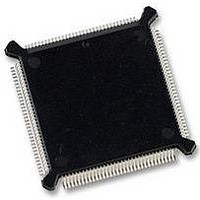
IC MCU 32BIT 25MHZ 132-PQFP
Manufacturer
Freescale Semiconductor
Series
M683xxr
Specifications of MC68331CEH25
Core Processor
CPU32
Core Size
32-Bit
Speed
25MHz
Connectivity
EBI/EMI, SCI, SPI, UART/USART
Peripherals
POR, PWM, WDT
Number Of I /o
18
Program Memory Type
ROMless
Voltage - Supply (vcc/vdd)
4.5 V ~ 5.5 V
Oscillator Type
Internal
Operating Temperature
-40°C ~ 85°C
Package / Case
132-QFP
Controller Family/series
68K
No. Of I/o's
18
Cpu Speed
25MHz
No. Of Timers
1
Embedded Interface Type
QSPI, SCI, UART
No. Of Pwm Channels
2
Digital Ic Case Style
PQFP
Rohs Compliant
Yes
Processor Series
M683xx
Core
CPU32
Data Bus Width
32 bit
Data Ram Size
80 B
Interface Type
QSPI, SCI, UART
Maximum Clock Frequency
25 MHz
Number Of Programmable I/os
18
Number Of Timers
1
Maximum Operating Temperature
+ 85 C
Mounting Style
SMD/SMT
Minimum Operating Temperature
- 40 C
Eeprom Size
-
Ram Size
-
Program Memory Size
-
Data Converters
-
Lead Free Status / Rohs Status
Details
Available stocks
Company
Part Number
Manufacturer
Quantity
Price
Company:

Part Number:
MC68331CEH25
Manufacturer:
PANASONIC
Quantity:
2 000
Company:
Part Number:
MC68331CEH25
Manufacturer:
Freescale Semiconductor
Quantity:
135
Company:
Part Number:
MC68331CEH25
Manufacturer:
Freescale Semiconductor
Quantity:
10 000


3.7.3 Reset Timing
3.7.4 Power-On Reset
38
The RESET input must be asserted for a specified minimum period in order for reset to occur. External
RESET assertion can be delayed internally for a period equal to the longest bus cycle time (or the bus
monitor time-out period) in order to protect write cycles from being aborted by reset. While RESET is
asserted, SIM pins are either in a disabled high-impedance state or are driven to their inactive states.
When an external device asserts RESET for the proper period, reset control logic clocks the signal into
an internal latch. The control logic drives the RESET pin low for an additional 512 CLKOUT cycles after
it detects that the RESET signal is no longer being externally driven, to guarantee this length of reset
to the entire system.
If an internal source asserts a reset signal, the reset control logic asserts RESET for a minimum of 512
cycles. If the reset signal is still asserted at the end of 512 cycles, the control logic continues to assert
RESET until the internal reset signal is negated.
After 512 cycles have elapsed, the reset input pin goes to an inactive, high-impedance state for 10 cy-
cles. At the end of this 10-cycle period, the reset input is tested. When the input is at logic level one,
reset exception processing begins. If, however, the reset input is at logic level zero, the reset control
logic drives the pin low for another 512 cycles. At the end of this period, the pin again goes to high-
impedance state for 10 cycles, then it is tested again. The process repeats until RESET is released.
When the SIM clock synthesizer is used to generate the system clock, power-on reset involves special
circumstances related to application of system and clock synthesizer power. Regardless of clock
source, voltage must be applied to clock synthesizer power input pin V
operate. The following discussion assumes that V
mizes crystal start-up time. When V
crystal parameters and by oscillator circuit design. V
During power-on reset, an internal circuit in the SIM drives the internal (IMB) and external reset lines.
The circuit releases the internal reset line as V
pins are initialized. When V
operation. Clock frequency ramps up to the specified limp mode frequency. The external RESET line
remains asserted until the clock synthesizer PLL locks and 512 CLKOUT cycles elapse.
Module
CPU32
QSM
GPT
Freescale Semiconductor, Inc.
For More Information On This Product,
DD
reaches the specified minimum value, the clock synthesizer VCO begins
Table 19 Module Pin Functions
Go to: www.freescale.com
DDSYN
PQS[6:4]/PCS[3:1]
PGP[6:3]/OC[4:1]
PGP[2:0]/IC[3:1]
PQS3/PCS0/SS
PGP7/IC4/OC5
Pin Mnemonic
PWMA, PWMB
BKPT/DSCLK
DSI/IFETCH
PQS1/MOSI
PQS0/MISO
DSO/IPIPE
PQS7/TXD
PQS2/SCK
PCLK
is applied at power-on, start-up time is affected by specific
RXD
PAI
DD
DDSYN
ramps up to the minimum specified value, and SIM
DD
ramp-up time also affects pin state during reset.
is applied before and during reset. This mini-
DDSYN
Discrete Output
BKPT/DSCLK
Discrete Input
Discrete Input
Discrete Input
Discrete Input
Discrete Input
Discrete Input
Discrete Input
Discrete Input
Discrete Input
Discrete Input
Discrete Input
DSI/IFETCH
DSO/IPIPE
Function
in order for the MCU to
RXD
MC68331TS/D
Related parts for MC68331CEH25
Image
Part Number
Description
Manufacturer
Datasheet
Request
R

Part Number:
Description:
Mc68331 32 Bit Microcontroller
Manufacturer:
Freescale Semiconductor, Inc
Datasheet:
Part Number:
Description:
Manufacturer:
Freescale Semiconductor, Inc
Datasheet:
Part Number:
Description:
Manufacturer:
Freescale Semiconductor, Inc
Datasheet:
Part Number:
Description:
Manufacturer:
Freescale Semiconductor, Inc
Datasheet:
Part Number:
Description:
Manufacturer:
Freescale Semiconductor, Inc
Datasheet:
Part Number:
Description:
Manufacturer:
Freescale Semiconductor, Inc
Datasheet:
Part Number:
Description:
Manufacturer:
Freescale Semiconductor, Inc
Datasheet:
Part Number:
Description:
Manufacturer:
Freescale Semiconductor, Inc
Datasheet:
Part Number:
Description:
Manufacturer:
Freescale Semiconductor, Inc
Datasheet:
Part Number:
Description:
Manufacturer:
Freescale Semiconductor, Inc
Datasheet:
Part Number:
Description:
Manufacturer:
Freescale Semiconductor, Inc
Datasheet:
Part Number:
Description:
Manufacturer:
Freescale Semiconductor, Inc
Datasheet:
Part Number:
Description:
Manufacturer:
Freescale Semiconductor, Inc
Datasheet:
Part Number:
Description:
Manufacturer:
Freescale Semiconductor, Inc
Datasheet:
Part Number:
Description:
Manufacturer:
Freescale Semiconductor, Inc
Datasheet: