MC68HC11K0CFUE4 Freescale Semiconductor, MC68HC11K0CFUE4 Datasheet - Page 40
MC68HC11K0CFUE4
Manufacturer Part Number
MC68HC11K0CFUE4
Description
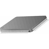
MCU 8-BIT 768 RAM 4MHZ 80-QFP
Manufacturer
Freescale Semiconductor
Series
HC11r
Specifications of MC68HC11K0CFUE4
Core Processor
HC11
Core Size
8-Bit
Speed
4MHz
Connectivity
SCI, SPI
Peripherals
POR, PWM, WDT
Number Of I /o
37
Program Memory Type
ROMless
Ram Size
768 x 8
Voltage - Supply (vcc/vdd)
4.5 V ~ 5.5 V
Data Converters
A/D 8x8b
Oscillator Type
Internal
Operating Temperature
-40°C ~ 85°C
Package / Case
80-QFP
Data Bus Width
8 bit
Data Ram Size
768 B
Interface Type
SCI, SPI
Maximum Clock Frequency
4 MHz
Number Of Programmable I/os
37
Number Of Timers
8
Maximum Operating Temperature
+ 85 C
Mounting Style
SMD/SMT
Minimum Operating Temperature
- 40 C
On-chip Adc
8 bit, 8 Channel
Lead Free Status / RoHS Status
Lead free / RoHS Compliant
Eeprom Size
-
Program Memory Size
-
Lead Free Status / Rohs Status
Details
Available stocks
Company
Part Number
Manufacturer
Quantity
Price
Company:

Part Number:
MC68HC11K0CFUE4
Manufacturer:
Freescale Semiconductor
Quantity:
10 000


Pin Description
Technical Data
40
Address: $0038
In single-chip and bootstrap modes, the MODA pin typically is grounded
and has no function after reset. In expanded and special test modes,
MODA is normally connected to V
and functions as the load instruction register (LIR) pin after reset. The
open-drain, active-low LIR output drives low during the first E-clock cycle
of each instruction (opcode fetch), providing a useful signal for system
debugging.
LIR can be driven high for a portion of each instruction cycle by setting
the LIRDV bit in the system configuration options 2 (OPT2) register (see
Figure 2-7
instructions and prevent false triggering in high-speed applications.
LIRDV — LIR Driven Bit
Reset:
Read:
Write:
PREVIOUS INSTRUCTION
Freescale Semiconductor, Inc.
For More Information On This Product,
0 = LIR not driven high
1 = LIR driven high for one quarter cycle to reduce transition time
1. STRCH is not available on K devices.
Figure 2-7. System Configuration Options 2 (OPT2)
LIRDV
LAST CYCLE OF
Bit 7
0
LIR
E
and
Go to: www.freescale.com
CWOM
Figure
Pin Description
6
0
STRCH
2-8). This feature can help detect consecutive
FIRST CYCLE OF NEW
INSTRUCTION
Figure 2-8. LIR Timing
5
0
(1)
OPCODE FETCH
IRVNE
Note: If LIRDV is not set, the pullup resistor may
—
DD
4
through a 4.7-k pullup resistor
not return the level to a logic 1 before
the next data fetch.
LSBF
3
0
SPR2
2
0
M68HC11K Family
XDV1
1
0
MOTOROLA
XDV0
Bit 0
0
Related parts for MC68HC11K0CFUE4
Image
Part Number
Description
Manufacturer
Datasheet
Request
R

Part Number:
Description:
MC68HC11 EEPROM Programming from a Personal Computer
Manufacturer:
Motorola / Freescale Semiconductor

Part Number:
Description:
Manufacturer:
Freescale Semiconductor, Inc
Datasheet:
Part Number:
Description:
Manufacturer:
Freescale Semiconductor, Inc
Datasheet:
Part Number:
Description:
Manufacturer:
Freescale Semiconductor, Inc
Datasheet:
Part Number:
Description:
Manufacturer:
Freescale Semiconductor, Inc
Datasheet:
Part Number:
Description:
Manufacturer:
Freescale Semiconductor, Inc
Datasheet:
Part Number:
Description:
Manufacturer:
Freescale Semiconductor, Inc
Datasheet:
Part Number:
Description:
Manufacturer:
Freescale Semiconductor, Inc
Datasheet:
Part Number:
Description:
Manufacturer:
Freescale Semiconductor, Inc
Datasheet:
Part Number:
Description:
Manufacturer:
Freescale Semiconductor, Inc
Datasheet:
Part Number:
Description:
Manufacturer:
Freescale Semiconductor, Inc
Datasheet:
Part Number:
Description:
Manufacturer:
Freescale Semiconductor, Inc
Datasheet:
Part Number:
Description:
Manufacturer:
Freescale Semiconductor, Inc
Datasheet:
Part Number:
Description:
Manufacturer:
Freescale Semiconductor, Inc
Datasheet:
Part Number:
Description:
Manufacturer:
Freescale Semiconductor, Inc
Datasheet: