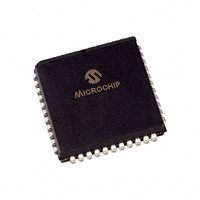
PIC16C74-04/L Microchip Technology, PIC16C74-04/L Datasheet - Page 79

PIC16C74-04/L
Manufacturer Part Number
PIC16C74-04/L
Description
MICRO CTRL 4K 4MHZ OTP 44PLCC
Manufacturer
Microchip Technology
Series
PIC® 16Cr
Datasheet
1.PIC16C72-04SO.pdf
(289 pages)
Specifications of PIC16C74-04/L
Core Processor
PIC
Core Size
8-Bit
Speed
4MHz
Connectivity
I²C, SPI, UART/USART
Peripherals
POR, PWM, WDT
Number Of I /o
33
Program Memory Size
7KB (4K x 14)
Program Memory Type
OTP
Ram Size
192 x 8
Voltage - Supply (vcc/vdd)
4 V ~ 6 V
Data Converters
A/D 8x8b
Oscillator Type
External
Operating Temperature
0°C ~ 70°C
Package / Case
44-PLCC
For Use With
DVA16XL441 - ADAPTER DEVICE ICE 44PLCC
Lead Free Status / RoHS Status
Request inventory verification / Request inventory verification
Eeprom Size
-
- Current page: 79 of 289
- Download datasheet (3Mb)
FIGURE 11-2: SSPCON: SYNC SERIAL PORT CONTROL REGISTER (ADDRESS 14h)
1997 Microchip Technology Inc.
bit7
bit 7:
bit 6:
bit 5:
bit 4:
bit 3-0: SSPM3:SSPM0: Synchronous Serial Port Mode Select bits
WCOL
R/W-0
WCOL: Write Collision Detect bit
1 = The SSPBUF register is written while it is still transmitting the previous word
(must be cleared in software)
0 = No collision
SSPOV: Receive Overflow Detect bit
In SPI mode
1 = A new byte is received while the SSPBUF register is still holding the previous data. In case of overflow,
the data in SSPSR register is lost. Overflow can only occur in slave mode. The user must read the SSP-
BUF, even if only transmitting data, to avoid setting overflow. In master mode the overflow bit is not set
since each new reception (and transmission) is initiated by writing to the SSPBUF register.
0 = No overflow
In I
1 = A byte is received while the SSPBUF register is still holding the previous byte. SSPOV is a "don’t care"
in transmit mode. SSPOV must be cleared in software in either mode.
0 = No overflow
SSPEN: Synchronous Serial Port Enable bit
In SPI mode
1 = Enables serial port and configures SCK, SDO, and SDI as serial port pins
0 = Disables serial port and configures these pins as I/O port pins
In I
1 = Enables the serial port and configures the SDA and SCL pins as serial port pins
0 = Disables serial port and configures these pins as I/O port pins
In both modes, when enabled, these pins must be properly configured as input or output.
CKP: Clock Polarity Select bit
In SPI mode
1 = Idle state for clock is a high level. Transmit happens on falling edge, receive on rising edge.
0 = Idle state for clock is a low level. Transmit happens on rising edge, receive on falling edge.
In I
SCK release control
1 = Enable clock
0 = Holds clock low (clock stretch) (Used to ensure data setup time)
0000 = SPI master mode, clock = Fosc/4
0001 = SPI master mode, clock = Fosc/16
0010 = SPI master mode, clock = Fosc/64
0011 = SPI master mode, clock = TMR2 output/2
0100 = SPI slave mode, clock = SCK pin. SS pin control enabled.
0101 = SPI slave mode, clock = SCK pin. SS pin control disabled. SS can be used as I/O pin.
0110 = I
0111 = I
1011 = I
1110 = I
1111 = I
SSPOV
R/W-0
2
2
2
C mode
C mode
C mode
2
2
2
2
2
C slave mode, 7-bit address
C slave mode, 10-bit address
C firmware controlled Master Mode (slave idle)
C slave mode, 7-bit address with start and stop bit interrupts enabled
C slave mode, 10-bit address with start and stop bit interrupts enabled
SSPEN
R/W-0
R/W-0
CKP
72 73 73A 74 74A 76 77
Applicable Devices
SSPM3
R/W-0
SSPM2
R/W-0
SSPM1
R/W-0
SSPM0
R/W-0
bit0
W = Writable bit
U = Unimplemented bit,
- n =Value at POR reset
R = Readable bit
read as ‘0’
PIC16C7X
DS30390E-page 79
Related parts for PIC16C74-04/L
Image
Part Number
Description
Manufacturer
Datasheet
Request
R

Part Number:
Description:
MICRO CTRL 4K 20MHZ OTP 44PLCC
Manufacturer:
Microchip Technology
Datasheet:

Part Number:
Description:
MICRO CTRL 4K 20MHZ OTP 40DIP
Manufacturer:
Microchip Technology
Datasheet:

Part Number:
Description:
MICRO CTRL 4K 10MHZ OTP ET 40DIP
Manufacturer:
Microchip Technology
Datasheet:

Part Number:
Description:
MICRO CTRL 4K 10MHZ OTP 40DIP
Manufacturer:
Microchip Technology
Datasheet:

Part Number:
Description:
MICRO CTRL 4K 4MHZ OTP 40DIP
Manufacturer:
Microchip Technology
Datasheet:

Part Number:
Description:
MICRO CTRL 4K 4MHZ OTP 40DIP
Manufacturer:
Microchip Technology
Datasheet:

Part Number:
Description:
MICRO CTRL 4K 20MHZ EPROM 40CDIP
Manufacturer:
Microchip Technology
Datasheet:

Part Number:
Description:
8-Bit CMOS Microcontrollers with A/D Converter
Manufacturer:
Microchip Technology

Part Number:
Description:
8-Bit CMOS Microcontrollers with A/D Converter
Manufacturer:
Microchip Technology

Part Number:
Description:
8-Bit CMOS Microcontrollers with A/D Converter
Manufacturer:
Microchip Technology

Part Number:
Description:
8-Bit CMOS Microcontrollers with A/D Converter
Manufacturer:
Microchip Technology

Part Number:
Description:
8-Bit CMOS Microcontrollers with A/D Converter
Manufacturer:
Microchip Technology

Part Number:
Description:
8-Bit CMOS Microcontrollers with A/D Converter
Manufacturer:
Microchip Technology

Part Number:
Description:
8-Bit CMOS Microcontrollers with A/D Converter
Manufacturer:
Microchip Technology

Part Number:
Description:
8-Bit CMOS Microcontrollers with A/D Converter
Manufacturer:
Microchip Technology


