AT90LS8535-4AI Atmel, AT90LS8535-4AI Datasheet - Page 76
AT90LS8535-4AI
Manufacturer Part Number
AT90LS8535-4AI
Description
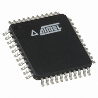
IC MCU 8K 4MHZ A/D LV IT 44TQFP
Manufacturer
Atmel
Series
AVR® 90LSr
Specifications of AT90LS8535-4AI
Core Processor
AVR
Core Size
8-Bit
Speed
4MHz
Connectivity
SPI, UART/USART
Peripherals
Brown-out Detect/Reset, POR, PWM, WDT
Number Of I /o
32
Program Memory Size
8KB (4K x 16)
Program Memory Type
FLASH
Eeprom Size
512 x 8
Ram Size
512 x 8
Voltage - Supply (vcc/vdd)
2.7 V ~ 6 V
Data Converters
A/D 8x10b
Oscillator Type
Internal
Operating Temperature
-40°C ~ 85°C
Package / Case
44-TQFP, 44-VQFP
Lead Free Status / RoHS Status
Contains lead / RoHS non-compliant
Available stocks
Company
Part Number
Manufacturer
Quantity
Price
Company:

Part Number:
AT90LS8535-4AI
Manufacturer:
Micron
Quantity:
1
Part Number:
AT90LS8535-4AI
Manufacturer:
ATMEL/爱特梅尔
Quantity:
20 000


I/O Ports
Port A
Port A Data Register – PORTA
Port A Data Direction Register
– DDRA
Port A Input Pins Address –
PINA
76
AT90S/LS8535
All AVR ports have true read-modify-write functionality when used as general digital I/O
ports. This means that the direction of one port pin can be changed without unintention-
ally changing the direction of any other pin with the SBI and CBI instructions. The same
applies for changing drive value (if configured as output) or enabling/disabling of pull-up
resistors (if configured as input).
Port A is an 8-bit bi-directional I/O port.
Three I/O memory address locations are allocated for Port A, one each for the Data
Register – PORTA, $1B($3B), Data Direction Register – DDRA, $1A($3A) and the Port
A Input Pins – PINA, $19($39). The Port A Input Pins address is read-only, while the
Data Register and the Data Direction Register are read/write.
All port pins have individually selectable pull-up resistors. The Port A output buffers can
sink 20 mA and thus drive LED displays directly. When pins PA0 to PA7 are used as
inputs and are externally pulled low, they will source current if the internal pull-up resis-
tors are activated.
Port A has an alternate function as analog inputs for the ADC. If some Port A pins are
configured as outputs, it is essential that these do not switch when a conversion is in
progress. This might corrupt the result of the conversion.
During Power-down mode, the Schmitt trigger of the digital input is disconnected. This
allows analog signals that are close to V
causing excessive power consumption.
The Port A Input Pins address (PINA) is not a register; this address enables access to
the physical value on each Port A pin. When reading PORTA, the Port A Data Latch is
read and when reading PINA, the logical values present on the pins are read.
Bit
$1B ($3B)
Read/Write
Initial Value
Bit
$1A ($3A)
Read/Write
Initial Value
Bit
$19 ($39)
Read/Write
Initial Value
PORTA7
PINA7
DDA7
R/W
R/W
N/A
R
7
0
7
0
7
PORTA6
PINA6
DDA6
R/W
R/W
N/A
R
6
0
6
0
6
PORTA5
PINA5
DDA5
R/W
R/W
N/A
R
5
0
5
0
5
PORTA4
PINA4
DDA4
R/W
R/W
N/A
R
4
0
4
0
4
CC
/2 to be present during power-down without
PORTA3
PINA3
DDA3
R/W
R/W
N/A
R
3
0
3
0
3
PORTA2
PINA2
DDA2
R/W
R/W
N/A
R
2
0
2
0
2
PORTA1
PINA1
DDA1
R/W
R/W
N/A
R
1
0
1
0
1
PORTA0
PINA0
DDA0
R/W
R/W
N/A
R
0
0
0
0
0
1041H–11/01
PORTA
DDRA
PINA
Related parts for AT90LS8535-4AI
Image
Part Number
Description
Manufacturer
Datasheet
Request
R

Part Number:
Description:
DEV KIT FOR AVR/AVR32
Manufacturer:
Atmel
Datasheet:

Part Number:
Description:
INTERVAL AND WIPE/WASH WIPER CONTROL IC WITH DELAY
Manufacturer:
ATMEL Corporation
Datasheet:
Part Number:
Description:
Low-Voltage Voice-Switched IC for Hands-Free Operation
Manufacturer:
ATMEL Corporation
Datasheet:
Part Number:
Description:
MONOLITHIC INTEGRATED FEATUREPHONE CIRCUIT
Manufacturer:
ATMEL Corporation
Datasheet:
Part Number:
Description:
AM-FM Receiver IC U4255BM-M
Manufacturer:
ATMEL Corporation
Datasheet:
Part Number:
Description:
Monolithic Integrated Feature Phone Circuit
Manufacturer:
ATMEL Corporation
Datasheet:
Part Number:
Description:
Multistandard Video-IF and Quasi Parallel Sound Processing
Manufacturer:
ATMEL Corporation
Datasheet:
Part Number:
Description:
High-performance EE PLD
Manufacturer:
ATMEL Corporation
Datasheet:
Part Number:
Description:
8-bit Flash Microcontroller
Manufacturer:
ATMEL Corporation
Datasheet:
Part Number:
Description:
2-Wire Serial EEPROM
Manufacturer:
ATMEL Corporation
Datasheet: