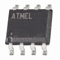
AT90S2323-10SC Atmel, AT90S2323-10SC Datasheet - Page 39

AT90S2323-10SC
Manufacturer Part Number
AT90S2323-10SC
Description
MCU 2K FLASH 10MHZ 8-SOIC
Manufacturer
Atmel
Series
AVR® 90Sr
Datasheet
1.AT90LS2323-4PC.pdf
(64 pages)
Specifications of AT90S2323-10SC
Core Processor
AVR
Core Size
8-Bit
Speed
10MHz
Connectivity
SPI
Peripherals
Brown-out Detect/Reset, POR, WDT
Number Of I /o
3
Program Memory Size
2KB (1K x 16)
Program Memory Type
FLASH
Eeprom Size
128 x 8
Ram Size
128 x 8
Voltage - Supply (vcc/vdd)
4 V ~ 6 V
Oscillator Type
Internal
Operating Temperature
0°C ~ 70°C
Package / Case
8-SOIC (5.3mm Width), 8-SOP, 8-SOEIAJ
Lead Free Status / RoHS Status
Contains lead / RoHS non-compliant
Data Converters
-
Available stocks
Company
Part Number
Manufacturer
Quantity
Price
Part Number:
AT90S2323-10SC
Manufacturer:
ATMEL/爱特梅尔
Quantity:
20 000
High-voltage Serial
Programming Algorithm
1004D–09/01
To program and verify the AT90S/LS2323 and AT90S/LS234 in the high-voltage Serial
Programming mode, the following sequence is recommended (see instruction formats in
Table 16):
1. Power-up sequence: Apply 4.5 - 5.5V between V
2. The Flash array is programmed one byte at a time by supplying first the address,
3. The EEPROM array is programmed one byte at a time by supplying first the
4. Any memory location can be verified by using the Read instruction, which returns
5. Power-off sequence:Set PB3 to “0”.
When writing or reading serial data to the device, data is clocked on the rising edge of
the serial clock. See Figure 33, Figure 34 and Table 17 for details.
Figure 33. High-voltage Serial Programming Waveforms
SERIAL DATA OUTPUT
SERIAL CLOCK INPUT
SERIAL INSTR. INPUT
SERIAL DATA INPUT
PB0 to “0” and wait at least 100 ns. Then, if the RCEN Fuse is not programmed,
toggle XTAL1/PB3 at least four times with minimum 100 ns pulse width. Set PB3
to “0”. Wait at least 100 ns. Or, if the RCEN Fuse is programmed, set PB3 to “0”.
Wait for least 4 µs. In both cases, apply 12V to RESET and wait at least 100 ns
before changing PB0. Wait 8 µs before giving any instructions.
then the low and high data bytes. The write instruction is self-timed; wait until the
PB2 (RDY/BSY) pin goes high.
address, then the data byte. The write instruction is self-timed; wait until the PB2
(RDY/BSY) pin goes high.
the contents at the selected address at serial output PB2.
Set RESET to “0”.
Turn V
CC
XTAL1/PB3
power off.
PB0
PB1
PB2
0
MSB
MSB
MSB
1
2
3
4
AT90S/LS2323/2343
5
CC
and GND. Set RESET and
6
7
LSB
LSB
LSB
8
9
10
39


