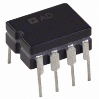
AD708AQ Analog Devices Inc, AD708AQ Datasheet - Page 11

AD708AQ
Manufacturer Part Number
AD708AQ
Description
IC OPAMP GP DUAL PREC 8CDIP
Manufacturer
Analog Devices Inc
Datasheet
1.AD708JNZ.pdf
(16 pages)
Specifications of AD708AQ
Slew Rate
0.3 V/µs
Rohs Status
RoHS non-compliant
Amplifier Type
General Purpose
Number Of Circuits
2
-3db Bandwidth
900kHz
Current - Input Bias
1nA
Voltage - Input Offset
30µV
Current - Supply
4.5mA
Voltage - Supply, Single/dual (±)
6 V ~ 36 V, ±3 V ~ 18 V
Operating Temperature
-40°C ~ 85°C
Mounting Type
Through Hole
Package / Case
8-CDIP (0.300", 7.62mm)
Op Amp Type
Low Offset Voltage
No. Of Amplifiers
2
Bandwidth
900kHz
Supply Voltage Range
± 3V To ± 18V
Amplifier Case Style
DIP
No. Of Pins
8
Output Type
-
Current - Output / Channel
-
Gain Bandwidth Product
-
Lead Free Status / RoHS Status
Contains lead / RoHS non-compliant
Available stocks
Company
Part Number
Manufacturer
Quantity
Price
OPERATION WITH A GAIN OF −100
To show the outstanding dc precision of the AD708 in a real
application, Table 3 shows an error budget calculation for a gain
of −100. This configuration is shown in Figure 28.
Table 3.
Error Sources
V
I
Gain (2 kΩ Load)
Noise
V
Total Unadjusted
With Offset
This error budget assumes no error in the resistor ratio and no
error from power supply variation (the 120 dB minimum PSRR
of the AD708S makes this a good assumption). The external
resistors can cause gain error from mismatch and drift over
temperature.
HIGH PRECISION PROGRAMMABLE GAIN
AMPLIFIER
The three op amp programmable gain amplifier shown in
Figure 29 takes advantage of the outstanding matching
characteristics of the AD708 to achieve high dc precision.
OS
OS
OS
Error
Calibrated Out
Drift
V
IN
Figure 28. Gain of −100 Configuration
1kΩ
1kΩ
Maximum Error Contribution
A
(Full Scale: V
30 μV/100 mV
(100 kΩ)(1 nA)/10 V
10 V/(5 × 106)/100 mV
0.35 mV/100 mV
(0.3 mV/°C)/100 mV
@ 25°C
−55°C to +125°C
@ 25°C
−55°C to +125°C
V
= 100 (S Grade)
100kΩ
2
3
–
+
AD708
1/2
OUT
+V
–V
7
4
S
S
= 10 V, V
0.1µF
0.1µF
6
IN
= 300 ppm
= 10 ppm
= 20 ppm
= 4 ppm
= 3 ppm/°C
= 334 ppm > 11 bits
= 634 ppm > 10 bits
= 34 ppm > 14 bits
= 334 ppm > 11 bits
= 100 mV)
V
OUT
Rev. C | Page 11 of 16
The gains of the circuit are controlled by the select lines, A0 and
A1, of the
this design.
The input stage attains very high dc precision due to the 30 μV
maximum offset voltage match of the AD708S and the 1 nA
maximum input bias current match. The accuracy is main-
tained over temperature because of the ultralow drift
performance of the AD708.
To achieve 0.1% gain accuracy, along with high common-mode
rejection, the circuit should be trimmed.
To maximize common-mode rejection
1.
2.
3.
4.
To minimize gain errors
1.
2.
3.
The design shown in Figure 29 should allow for 0.1% gain
accuracy and 0.1 μV/V common-mode rejection when ±1%
resistors and ±5% potentiometers are used.
–V
+V
A0
A1
V
V
INA
S
S
INB
Set the select lines for gain = 1 and ground V
Apply a precision dc voltage to V
V
Connect V
the full-scale common mode expected.
Trim R
Select gain = 10 with the control lines and apply a
differential input voltage.
Adjust the 100 Ω potentiometer to V
(adjust V
Repeat Step 1 and Step 2 for gain = 100 and gain = 1000,
adjusting the 1 kΩ and 10 kΩ potentiometers, respectively.
O
OUT
OUT
= −V
1–4
5–8
AD7502
AD7502
AD708
AD708
B
1/2
1/2
B
S1
S2
S3
S4
S8
S7
S6
S5
until V
INA
IN
INB
magnitude as necessary).
100Ω
to the required precision.
to V
multiplexer, and are 1, 10, 100, and 1000 in
O
10kΩ
10kΩ
Figure 29. Precision PGA
= 0 V.
INA
1kΩ
and apply an input voltage equal to
10kΩ
10kΩ
10kΩ
INA
10kΩ
10kΩ
and trim R
O
= 10 V
10kΩ
10kΩ
INB
IN
9.9kΩ
9.9kΩ
R
B
A
.
AD707
until
AD708
R
A


