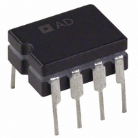
AD708AQ Analog Devices Inc, AD708AQ Datasheet - Page 12

AD708AQ
Manufacturer Part Number
AD708AQ
Description
IC OPAMP GP DUAL PREC 8CDIP
Manufacturer
Analog Devices Inc
Datasheet
1.AD708JNZ.pdf
(16 pages)
Specifications of AD708AQ
Slew Rate
0.3 V/µs
Rohs Status
RoHS non-compliant
Amplifier Type
General Purpose
Number Of Circuits
2
-3db Bandwidth
900kHz
Current - Input Bias
1nA
Voltage - Input Offset
30µV
Current - Supply
4.5mA
Voltage - Supply, Single/dual (±)
6 V ~ 36 V, ±3 V ~ 18 V
Operating Temperature
-40°C ~ 85°C
Mounting Type
Through Hole
Package / Case
8-CDIP (0.300", 7.62mm)
Op Amp Type
Low Offset Voltage
No. Of Amplifiers
2
Bandwidth
900kHz
Supply Voltage Range
± 3V To ± 18V
Amplifier Case Style
DIP
No. Of Pins
8
Output Type
-
Current - Output / Channel
-
Gain Bandwidth Product
-
Lead Free Status / RoHS Status
Contains lead / RoHS non-compliant
Available stocks
Company
Part Number
Manufacturer
Quantity
Price
AD708
BRIDGE SIGNAL CONDITIONER
The AD708 can be used in the circuit shown in Figure 30 to
produce an accurate and inexpensive dynamic bridge condi-
tioner. The low offset voltage match and low offset voltage drift
match of the AD708 combine to achieve circuit performance
better than all but the best instrumentation amplifiers. The
outstanding specifications of the AD708, such as open-loop
gain, input offset currents, and low input bias currents, do not
limit circuit accuracy.
As configured, the circuit only requires a gain resistor, R
suitable accuracy and a stable, accurate voltage reference. The
transfer function is
The only significant errors due to the AD708S are
To achieve high accuracy, Resistor R
with a low drift coefficient.
PRECISION ABSOLUTE VALUE CIRCUIT
The AD708 is ideally suited to the precision absolute value
circuit shown in Figure 31. The low offset voltage match of the
V
V
V
V
IN
O
OS_OUT
OS_OUT
= V
AD580
REF
+15V
V
10kΩ
(T) = (V
= (V
REF
2.5V
Figure 30. Bridge Signal Conditioning Circuit
5kΩ
Figure 31. Precision Absolute Value Circuit
[ΔR/(R + ΔR)][R
OS_MATCH
OS_DRIFT
R
R
AD708
–15V
10kΩ
1/2
)(2R
IN459
NOTE
1
887Ω
LOW LEAKAGE DIODES
10kΩ
)(2R
R = 350Ω
R + ΔR
1
G
/R) = 30 mV
G
G
IN459
/R) = 0.3 mV/°C
5kΩ
/R]
3.75kΩ
G
1
should be 0.1% or better
175kΩ
R
AD708
AD708
10kΩ
G
AD708
1/2
1/2
1/2
V
O
V
O
= |V
G
, of
IN
|
Rev. C | Page 12 of 16
AD708 enables this circuit to accurately resolve the input signal.
In addition, the tight offset voltage drift match maintains the
resolution of the circuit over the full military temperature
range. The high dc open-loop gain and exceptional gain
linearity allows the circuit to perform well at both large and
small signal levels.
In this circuit, the only significant dc errors are due to the offset
voltage of the two amplifiers, the input offset current match of
the amplifiers, and the mismatch of the resistors. Errors
associated with the AD708S contribute less than 0.001% error
over −55°C to +125°C.
Maximum error at 25°C
Maximum error at +125°C or −55°C
Figure 32 shows V
signal at 0.05 Hz. Note that the circuit exhibits very low offset at
the zero crossing. This circuit can also produce V
reversing the polarity of the two diodes.
SELECTION OF PASSIVE COMPONENTS
Use high quality passive components to take full advantage of
the high precision and low drift characteristics of the AD708.
Discrete resistors and resistor networks with temperature
coefficients of less than 10 ppm/°C are available from Vishay,
Caddock, Precision Replacement Parts (PRP), and others.
30
50
μV
μV
+
+
Figure 32. Absolute Value Circuit Performance
10
(
(
10
10
2
1mV
nA
V
V
kΩ
OUT
)(
)(
10
1
vs. V
(Input Signal = 0.05 Hz)
nA
kΩ
)
)
V
IN
=
=
IN
40
for this circuit with a ±3 mV input
7
= 1mV/DIV
ppm
μV/10
@
μV
+
125
=
4
°
C
1mV
ppm
OUT
= −|V
IN
| by


