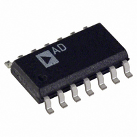
AD8040AR Analog Devices Inc, AD8040AR Datasheet - Page 17

AD8040AR
Manufacturer Part Number
AD8040AR
Description
IC AMP GP R-R QUAD LP 14SOIC
Manufacturer
Analog Devices Inc
Datasheet
1.AD8029ARZ.pdf
(20 pages)
Specifications of AD8040AR
Rohs Status
RoHS non-compliant
Amplifier Type
General Purpose
Number Of Circuits
4
Output Type
Rail-to-Rail
Slew Rate
63 V/µs
-3db Bandwidth
125MHz
Current - Input Bias
1.7µA
Voltage - Input Offset
2000µV
Current - Supply
1.4mA
Current - Output / Channel
170mA
Voltage - Supply, Single/dual (±)
2.7 V ~ 12 V, ±1.35 V ~ 6 V
Operating Temperature
-40°C ~ 125°C
Mounting Type
Surface Mount
Package / Case
14-SOIC (3.9mm Width), 14-SOL
Gain Bandwidth Product
-
Available stocks
Company
Part Number
Manufacturer
Quantity
Price
Part Number:
AD8040AR
Manufacturer:
ADI/亚德诺
Quantity:
20 000
Part Number:
AD8040ARUZ
Manufacturer:
ADI/亚德诺
Quantity:
20 000
Company:
Part Number:
AD8040ARZ
Manufacturer:
ADI
Quantity:
150
Part Number:
AD8040ARZ
Manufacturer:
ADI/亚德诺
Quantity:
20 000
Table 5. Effect of Load on Performance
Noninverting
Gain
1
1
1
2
2
2
–1
–1
–1
The feedback resistance (R
capacitance to form a pole in the amplifier’s loop response. This
can cause peaking and ringing in the amplifier’s response if the
RC time constant is too low. Figure 55 illustrates this effect.
Peaking can be reduced by adding a small capacitor (1 pF–4 pF)
across the feedback resistor. The best way to find the optimal
value of capacitor is to empirically try it in your circuit. Another
factor of higher resistance values is the impact it has on noise
performance. Higher resistor values generate more noise. Each
application is unique and therefore a balance must be reached
between distortion, peaking, and noise performance. Table 5
outlines the trade-offs that different loads have on distortion,
peaking, and noise performance. In gains of 1, 2, and 10,
equivalent loads of 1 kΩ, 2 kΩ, and 5 kΩ are shown.
With increasing load resistance, the distortion and –3 dB
bandwidth improve, while the noise and peaking degrade
slightly.
Figure 55. Frequency Response for Various Feedback/Load Resistances
–1
–2
–3
–4
–5
–6
–7
–8
2
1
0
1
V
V
S
OUT
= 5V
= 0.1V p-p
R
R
F
F
= R
= R
R
(kΩ)
0
0
0
1
2.5
5
1
2.5
5
L
L
F
= 2.5kΩ
= 1kΩ
10
FREQUENCY (MHz)
G = +2
F
|| R
R
(kΩ)
N/A
N/A
N/A
1
2.5
5
1
2.5
5
G
G
) combines with the input
R
F
= R
R
(kΩ)
1
2
5
1
2.5
5
1
2.5
5
100
LOAD
L
= 5kΩ
R
L
R
R
= 1kΩ
L
L
G = +1
= 2.5kΩ
= 5kΩ
–3 dB SS BW
(MHz)
120
130
139
36
44.5
43
40
40
34
1000
Rev. A | Page 17 of 20
Peaking
(dB)
0.02
0.6
1
0
0.2
2
0.01
0.05
1
DISABLE PIN
The AD8029 disable pin allows the amplifier to be shut down
for power conservation or multiplexing applications. When in
the disable mode, the amplifier draws only 150 µA of quiescent
current. The disable pin control voltage is referenced to the
negative supply. The amplifier enters power-down mode any
time the disable pin is tied to the most negative supply or within
0.8 V of the negative supply. If left open, the amplifier will
operate normally. For switching levels, refer to Table 6.
Table 6. Disable Pin Control Voltage
Disable Pin
Voltage
Low
(Disabled)
High
(Enabled)
HD2 at 1 MHz,
2 V p-p (dB)
–80
–84
–87.5
–72
–79
–84
–68
–74
–78
+3 V
0 V to <0.8 V
1.2 V to 3 V
AD8029/AD8030/AD8040
HD3 at 1 MHz,
2 V p-p (dB)
–72
–83
–92.5
–60
–72.5
–86
–57
–68
–80
Supply Voltage
+5 V
0 V to <0.8 V
1.2 V to 5 V
Output Noise
(nV/√Hz)
16.5
16.5
16.5
33.5
34.4
36
33.6
34
36
±5 V
–5 V to <–4 .2 V
–3.8 V to +5 V


