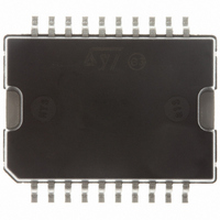
L4925PD STMicroelectronics, L4925PD Datasheet

L4925PD
Specifications of L4925PD
Available stocks
Related parts for L4925PD
L4925PD Summary of contents
Page 1
... It is designed for supplying microcomputer controlled systems especially in automotive applications. Table 1. Device summary Package PowerSO-20 Doc ID 1770 Rev 7 L4925 Order codes Tube Tape and reel L4925PD L4925PD013TR 1/14 www.st.com 1 ...
Page 2
Contents Contents 1 Block and pin connections diagrams . . . . . . . . . . . . . . . . . . . . . . . . . . . 5 1.1 Thermal data . ...
Page 3
L4925 List of tables Table 2. Thermal data ...
Page 4
List of figures List of figures Figure 1. Block diagram . . . . . . . . . . . . . . . . . . . . . . . . . . . . . . ...
Page 5
L4925 1 Block and pin connections diagrams Figure 1. Block diagram PREREGULATOR GND REG Figure 2. PowerSO-20 pin connections (top view) 1.1 Thermal data Table 2. Thermal data Symbol R Thermal resistance junction to ambient th(j-amb) ...
Page 6
Electrical specifications 2 Electrical specifications 2.1 Absolute maximum ratings Table 3. Absolute maximum ratings Symbol V DC operating supply voltage SDC V Transient supply voltage (t < 1s) STR I Output current O V Output voltage O V Output voltage ...
Page 7
L4925 Table 4. Electrical characteristics (continued) Symbol Parameter Reset V Reset threshold voltage RT V Reset threshold RTH t Reset pulse delay RD t Reset reaction time RR V Reset output low voltage RL Reset output high leakage I RH ...
Page 8
Functional description 3 Functional description The L4925 is a monolithic integrated voltage regulator, based on the STM modular voltage regulator approach. Several outstanding features and auxiliary functions are implemented to meet the requirements of supplying microprocessor systems in automotive applications. ...
Page 9
L4925 Figure 4. Output voltage vs input voltage Figure 5. Quiescent current vs supply voltage 3.2 Reset circuit The block circuit diagram of the reset circuit is shown in supervises the output voltage. The reset threshold of 4 ...
Page 10
Functional description Figure 6. Block circuit diagram Figure 7. Reset output waveforms 10/14 Doc ID 1770 Rev 7 L4925 ...
Page 11
L4925 4 Application information 4.1 Supply voltage transients High supply voltage transients can cause a reset output signal disturbance. For supply voltage greater than 8 V the circuit shows a high immunity of the reset output against supply transients of ...
Page 12
Package Informations 5 Package Informations Figure 9. PowerSO-20 mechanical data and package dimensions mm DIM. MIN. TYP. MAX. A 3.6 a1 0.1 0 0.1 b 0.4 0.53 c 0.23 0.32 D (1) 15 (2) ...
Page 13
L4925 6 Revision history Table 5. Document revision history Date 01-Oct-2003 18-Nov-2005 03-Feb-2006 09-Feb-2010 Revision 4 First issue in EDOCD DMS Added GND pins to fig Added order code and changed the formatting style in compliance with the ...
Page 14
... Information in this document is provided solely in connection with ST products. STMicroelectronics NV and its subsidiaries (“ST”) reserve the right to make changes, corrections, modifications or improvements, to this document, and the products and services described herein at any time, without notice. All ST products are sold pursuant to ST’s terms and conditions of sale. ...


