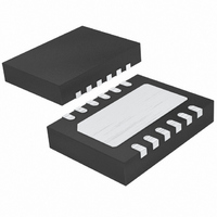
LT4356HDE-3#PBF Linear Technology, LT4356HDE-3#PBF Datasheet - Page 4

LT4356HDE-3#PBF
Manufacturer Part Number
LT4356HDE-3#PBF
Description
IC REG OVP W/LATCHOFF 12DFN
Manufacturer
Linear Technology
Datasheet
1.LT4356HDE-3PBF.pdf
(24 pages)
Specifications of LT4356HDE-3#PBF
Voltage - Working
4 ~ 80V
Voltage - Clamping
27V Adj
Technology
Mixed Technology
Number Of Circuits
1
Applications
Automotive
Package / Case
12-DFN
Input Voltage
1.25V
Internal Switch
No
Supply Voltage Range
4V To 80V
Digital Ic Case Style
DFN
No. Of Pins
12
Operating Temperature Range
-40°C To +125°C
Msl
MSL 1 - Unlimited
Rohs Compliant
Yes
Lead Free Status / RoHS Status
Lead free / RoHS Compliant
Power (watts)
-
ELECTRICAL CHARACTERISTICS
LT4356-3
temperature range, otherwise specifi cations are at T
SYMBOL
I
ΔV
V
V
I
t
t
Note 1: Stresses beyond those listed under Absolute Maximum Ratings
may cause permanent damage to the device. Exposure to any Absolute
Maximum Rating condition for extended periods may affect device
reliability and lifetime.
Note 2: All currents into device pins are positive; all currents out of device
pins are negative. All voltages are referenced to GND unless otherwise
specifi ed.
TYPICAL PERFORMANCE CHARACTERISTICS
Specifi cations are at V
4
OUT
SHDN
OFF(OC
OFF(OV)
SHDN
SHDN(FLT)
OUT
1000
800
600
400
200
0
)
0
I
CC
PARAMETER
OUT Pin Input Current
OUT Pin High Threshold
SHDN Pin Threshold
SHDN Pin Float Voltage
SHDN Pin Current
Overcurrent Turn Off Delay Time
Overvoltage Turn Off Delay Time
10
vs V
CC
20
30
V
CC
CC
40
(V)
= 12V, T
50
60
A
= 25°C unless otherwise noted.
70
43563 G02
80
CONDITIONS
V
V
ΔV
V
V
V
GATE From High to Low, ΔV
GATE From High to Low, V
OUT
OUT
CC
CC
SHDN
OUT
= 12V to 48V
= 12V to 48V
= V
= V
= 0V
= V
60
50
40
30
20
10
CC
CC
0
CC
A
0
I
= 12V
= 12V, V
CC
= 25°C. V
– V
10
(Shutdown) vs V
OUT
The
SHDN
; EN From Low to High
20
l
CC
30
= 0V
denotes the specifi cations which apply over the full operating
FB
= 12V unless otherwise noted.
V
SNS
= 0 → 1.5V
CC
40
Note 3: An internal clamp limits the GATE pin to a minimum of 10V above
the OUT pin. Driving this pin to voltages beyond the clamp may damage
the device.
(V)
= 0 → 120mV
CC
50
60
70
43563 G01
80
l
l
l
l
l
l
l
l
35
30
25
20
15
10
5
0
–50
I
CC
MIN
0.25
(Shutdown) vs Temperature
0.6
0.4
0.6
–25
–1
0
TEMPERATURE (°C)
0.25
TYP
200
0.5
1.4
1.2
–4
25
6
2
50
MAX
300
0.7
1.7
2.1
2.1
14
–8
4
1
75
100
43563 G03
UNITS
43563fa
125
mA
μA
μA
μs
μs
V
V
V
V


