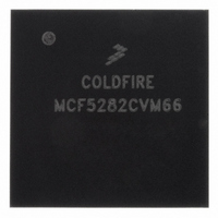
MCF5282CVM66 Freescale Semiconductor, MCF5282CVM66 Datasheet - Page 42

MCF5282CVM66
Manufacturer Part Number
MCF5282CVM66
Description
IC MPU 512K 66MHZ 256-MAPBGA
Manufacturer
Freescale Semiconductor
Series
MCF528xr
Datasheet
1.MCF5216CVM66J.pdf
(766 pages)
Specifications of MCF5282CVM66
Core Processor
Coldfire V2
Core Size
32-Bit
Speed
66MHz
Connectivity
CAN, EBI/EMI, Ethernet, I²C, SPI, UART/USART
Peripherals
DMA, LVD, POR, PWM, WDT
Number Of I /o
150
Program Memory Size
512KB (512K x 8)
Program Memory Type
FLASH
Ram Size
64K x 8
Voltage - Supply (vcc/vdd)
2.7 V ~ 3.6 V
Data Converters
A/D 8x10b
Oscillator Type
External
Operating Temperature
-40°C ~ 85°C
Package / Case
256-MAPBGA
Controller Family/series
ColdFire
No. Of I/o's
150
Ram Memory Size
64KB
Cpu Speed
66.67MHz
Embedded Interface Type
CAN, I2C, SPI, UART
No. Of Pwm Channels
8
Rohs Compliant
Yes
Lead Free Status / RoHS Status
Lead free / RoHS Compliant
Eeprom Size
-
Available stocks
Company
Part Number
Manufacturer
Quantity
Price
Company:
Part Number:
MCF5282CVM66
Manufacturer:
FREESCAL
Quantity:
152
Company:
Part Number:
MCF5282CVM66
Manufacturer:
Freescale Semiconductor
Quantity:
10 000
Part Number:
MCF5282CVM66
Manufacturer:
NXP/恩智浦
Quantity:
20 000
Company:
Part Number:
MCF5282CVM66J
Manufacturer:
Freescale Semiconductor
Quantity:
10 000
- Current page: 42 of 766
- Download datasheet (9Mb)
Overview
1.1.8
The SDRAM controller provides all required signals for glueless interfacing to a variety of
JEDEC-compliant SDRAM devices. SRAS/SCAS address multiplexing is software configurable for
different page sizes. To maintain refresh capability without conflicting with concurrent accesses on the
address and data buses, SRAS, SCAS, DRAMW, SDRAM_CS[1:0], and SCKE are dedicated SDRAM
signals.
1.1.9
The MCF5282 supports circuit board test strategies based on the Test Technology Committee of IEEE and
the Joint Test Action Group (JTAG). The test logic includes a test access port (TAP) consisting of a 16-state
controller, an instruction register, and three test registers (a 1-bit bypass register, a 256-bit boundary-scan
register, and a 32-bit ID register). The boundary scan register links the device’s pins into one shift register.
Test logic, implemented using static logic design, is independent of the device system logic.
The MCF5282 implementation supports the following:
1.1.10
The MCF5282 contains three full-duplex UARTs that function independently. The three UARTs can be
clocked by the system clock, eliminating the need for an external crystal.
Each UART has the following features:
1-10
•
•
•
•
•
•
•
•
•
•
•
•
•
•
•
•
•
•
Perform boundary-scan operations to test circuit board electrical continuity
Sample MCF5282 system pins during operation and transparently shift out the result in the
boundary scan register
Bypass the MCF5282 for a given circuit board test by effectively reducing the boundary-scan
register to a single bit
Disable the output drive to pins during circuit-board testing
Drive output pins to stable levels
Each can be clocked by the system clock, eliminating a need for an external UART clock
Full-duplex asynchronous/synchronous receiver/transmitter channel
Quadruple-buffered receiver
Double-buffered transmitter
Independently programmable receiver and transmitter clock sources
Programmable data format:
— 5–8 data bits plus parity
— Odd, even, no parity, or force parity
— One, one-and-a-half, or two stop bits
Each channel programmable to normal (full-duplex), automatic echo, local loop-back, or remote
loop-back mode
Automatic wake-up mode for multidrop applications
Four maskable interrupt conditions
All three UARTs have DMA request capability
Parity, framing, and overrun error detection
False-start bit detection
Line-break detection and generation
SDRAM Controller
Test Access Port
UART Modules
MCF5282 and MCF5216 ColdFire Microcontroller User’s Manual, Rev. 3
Freescale Semiconductor
Related parts for MCF5282CVM66
Image
Part Number
Description
Manufacturer
Datasheet
Request
R
Part Number:
Description:
Mcf5282 And Mcf5216 Coldfire Microcontroller User�s Manual
Manufacturer:
Freescale Semiconductor, Inc
Datasheet:
Part Number:
Description:
Manufacturer:
Freescale Semiconductor, Inc
Datasheet:
Part Number:
Description:
Manufacturer:
Freescale Semiconductor, Inc
Datasheet:
Part Number:
Description:
Manufacturer:
Freescale Semiconductor, Inc
Datasheet:
Part Number:
Description:
Manufacturer:
Freescale Semiconductor, Inc
Datasheet:
Part Number:
Description:
Manufacturer:
Freescale Semiconductor, Inc
Datasheet:
Part Number:
Description:
Manufacturer:
Freescale Semiconductor, Inc
Datasheet:
Part Number:
Description:
Manufacturer:
Freescale Semiconductor, Inc
Datasheet:
Part Number:
Description:
Manufacturer:
Freescale Semiconductor, Inc
Datasheet:
Part Number:
Description:
Manufacturer:
Freescale Semiconductor, Inc
Datasheet:
Part Number:
Description:
Manufacturer:
Freescale Semiconductor, Inc
Datasheet:
Part Number:
Description:
Manufacturer:
Freescale Semiconductor, Inc
Datasheet:
Part Number:
Description:
Manufacturer:
Freescale Semiconductor, Inc
Datasheet:
Part Number:
Description:
Manufacturer:
Freescale Semiconductor, Inc
Datasheet:
Part Number:
Description:
Manufacturer:
Freescale Semiconductor, Inc
Datasheet:


