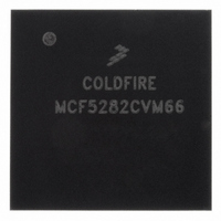
MCF5282CVM66 Freescale Semiconductor, MCF5282CVM66 Datasheet - Page 673

MCF5282CVM66
Manufacturer Part Number
MCF5282CVM66
Description
IC MPU 512K 66MHZ 256-MAPBGA
Manufacturer
Freescale Semiconductor
Series
MCF528xr
Datasheet
1.MCF5216CVM66J.pdf
(766 pages)
Specifications of MCF5282CVM66
Core Processor
Coldfire V2
Core Size
32-Bit
Speed
66MHz
Connectivity
CAN, EBI/EMI, Ethernet, I²C, SPI, UART/USART
Peripherals
DMA, LVD, POR, PWM, WDT
Number Of I /o
150
Program Memory Size
512KB (512K x 8)
Program Memory Type
FLASH
Ram Size
64K x 8
Voltage - Supply (vcc/vdd)
2.7 V ~ 3.6 V
Data Converters
A/D 8x10b
Oscillator Type
External
Operating Temperature
-40°C ~ 85°C
Package / Case
256-MAPBGA
Controller Family/series
ColdFire
No. Of I/o's
150
Ram Memory Size
64KB
Cpu Speed
66.67MHz
Embedded Interface Type
CAN, I2C, SPI, UART
No. Of Pwm Channels
8
Rohs Compliant
Yes
Lead Free Status / RoHS Status
Lead free / RoHS Compliant
Eeprom Size
-
Available stocks
Company
Part Number
Manufacturer
Quantity
Price
Company:
Part Number:
MCF5282CVM66
Manufacturer:
FREESCAL
Quantity:
152
Company:
Part Number:
MCF5282CVM66
Manufacturer:
Freescale Semiconductor
Quantity:
10 000
Part Number:
MCF5282CVM66
Manufacturer:
NXP/恩智浦
Quantity:
20 000
Company:
Part Number:
MCF5282CVM66J
Manufacturer:
Freescale Semiconductor
Quantity:
10 000
- Current page: 673 of 766
- Download datasheet (9Mb)
31.5.3.8 CLAMP Instruction
The CLAMP instruction selects the bypass register and asserts internal reset while simultaneously forcing
all output pins and bidirectional pins configured as outputs to the fixed values that are preloaded and held
in the boundary scan update register. CLAMP enhances test efficiency by reducing the overall shift path
to a single bit (the bypass register) while conducting an EXTEST type of instruction through the boundary
scan register.
31.5.3.9 BYPASS Instruction
The BYPASS instruction selects the bypass register, creating a single-bit shift register path from the TDI
pin to the TDO pin. BYPASS enhances test efficiency by reducing the overall shift path when a device
other than the ColdFire processor is the device under test on a board design with multiple chips on the
overall boundary scan chain. The shift register LSB is forced to logic 0 on the rising edge of TCLK after
entry into the capture-DR state. Therefore, the first bit shifted out after selecting the bypass register is
always logic 0. This differentiates parts that support an IDCODE register from parts that support only the
bypass register.
31.6
31.6.1
The test logic is a static logic design, and TCLK can be stopped in either a high or low state without loss
of data. However, the system clock is not synchronized to TCLK internally. Any mixed operation using
both the test logic and the system functional logic requires external synchronization.
Using the EXTEST instruction requires a circuit-board test environment that avoids device-destructive
configurations in which MCU output drivers are enabled into actively driven networks.
Low-power stop mode considerations:
31.6.2
Keeping the TAP controller in the test-logic-reset state ensures that the scan chain test logic is transparent
to the system logic. It is recommended that TMS, TDI, TCLK, and TRST be pulled up. TRST could be
connected to ground. However, since there is a pull-up on TRST, some amount of current results. The
internal power-on reset input initializes the TAP controller to the test-logic-reset state on power-up without
asserting TRST.
Freescale Semiconductor
•
•
•
The TAP controller must be in the test-logic-reset state to either enter or remain in the low-power
stop mode. Leaving the test-logic-reset state negates the ability to achieve low-power, but does not
otherwise affect device functionality.
The TCLK input is not blocked in low-power stop mode. To consume minimal power, the TCLK
input should be externally connected to V
The TMS, TDI, and TRST pins include on-chip pull-up resistors. For minimal power consumption
in low-power stop mode, these three pins should be either connected to V
Initialization/Application Information
Restrictions
Nonscan Chain Operation
MCF5282 and MCF5216 ColdFire Microcontroller User’s Manual, Rev. 3
DD
.
IEEE 1149.1 Test Access Port (JTAG)
DD
or left unconnected.
31-9
Related parts for MCF5282CVM66
Image
Part Number
Description
Manufacturer
Datasheet
Request
R
Part Number:
Description:
Mcf5282 And Mcf5216 Coldfire Microcontroller User�s Manual
Manufacturer:
Freescale Semiconductor, Inc
Datasheet:
Part Number:
Description:
Manufacturer:
Freescale Semiconductor, Inc
Datasheet:
Part Number:
Description:
Manufacturer:
Freescale Semiconductor, Inc
Datasheet:
Part Number:
Description:
Manufacturer:
Freescale Semiconductor, Inc
Datasheet:
Part Number:
Description:
Manufacturer:
Freescale Semiconductor, Inc
Datasheet:
Part Number:
Description:
Manufacturer:
Freescale Semiconductor, Inc
Datasheet:
Part Number:
Description:
Manufacturer:
Freescale Semiconductor, Inc
Datasheet:
Part Number:
Description:
Manufacturer:
Freescale Semiconductor, Inc
Datasheet:
Part Number:
Description:
Manufacturer:
Freescale Semiconductor, Inc
Datasheet:
Part Number:
Description:
Manufacturer:
Freescale Semiconductor, Inc
Datasheet:
Part Number:
Description:
Manufacturer:
Freescale Semiconductor, Inc
Datasheet:
Part Number:
Description:
Manufacturer:
Freescale Semiconductor, Inc
Datasheet:
Part Number:
Description:
Manufacturer:
Freescale Semiconductor, Inc
Datasheet:
Part Number:
Description:
Manufacturer:
Freescale Semiconductor, Inc
Datasheet:
Part Number:
Description:
Manufacturer:
Freescale Semiconductor, Inc
Datasheet:


