CGH40180PP-TB Cree Inc, CGH40180PP-TB Datasheet
CGH40180PP-TB
Specifications of CGH40180PP-TB


Related parts for CGH40180PP-TB


CGH40180PP-TB Summary of contents
Page 1
... CGH40180PP 180 W, RF Power GaN HEMT Cree’s CGH40180PP is an unmatched, gallium nitride (GaN) high electron mobility transistor (HEMT). The CGH40180PP, operating from a 28 volt rail, offers a general purpose, broadband solution to a variety of RF and microwave applications. GaN HEMTs offer high efficiency, high gain and wide bandwidth capabilities making the CGH40180PP ideal for linear and compressed amplifier circuits ...
Page 2
... Drain Efficiency 6 Output Mismatch Stress VSWR Dynamic Characteristics 7 Input Capacitance C Output Capacitance C Feedback Capacitance C Notes: Measured on wafer prior to packaging. 1 Scaled from PCM data. 2 Measured in CGH40180PP-TB, including all coupler losses 2 biasing each device at 1 defined as 2.8 mA. 5 SAT G Drain Efficiency = OUT DC Capacitance values are for each side of the device. ...
Page 3
... 800 900 Output Power and Drain Efficiency vs Frequency of the CGH40180PP measured in Broadband Amplifier Circuit CGH40180PP-TB 250 235 220 205 190 175 160 145 130 115 100 1100 Copyright © 2009-2011 Cree, Inc. All rights reserved. The information in this document is subject to change without notice. Cree and the Cree logo are registered trademarks of Cree, Inc ...
Page 4
... Typical Performance Gain and Drain Efficiency vs Output Power of the CGH40180PP in Broadband Amplifier Circuit CGH40180PP-TB 22 gain 1100 20 eff 1100 18 Gain Copyright © 2009-2011 Cree, Inc. All rights reserved. The information in this document is subject to change without notice. Cree and the Cree logo are registered trademarks of Cree, Inc. ...
Page 5
... Typical Performance Simulated Maximum Available Gain and K Factor of the CGH40180PP Typical Noise Performance Simulated Minimum Noise Figure and Noise Resistance vs Frequency of the CGH40180PP Electrostatic Discharge (ESD) Classifications Parameter Human Body Model Charge Device Model Copyright © 2009-2011 Cree, Inc. All rights reserved. The information in this document is subject to change without notice. Cree and the Cree logo are registered trademarks of Cree, Inc ...
Page 6
... Note 1. Area exceeds Maximum Case Operating Temperature (See Page 2). CGH40180PP Transient Power Dissipation De-rating Curve CGH40180PP Transient Power Dissipation De-Rating Curve 250 200 150 100 Note 1. Area exceeds Maximum Case Operating Temperature (See Page 2). Note 2. This transient de-rating curve assumes a 1msec pulse with a 20% duty cycle with no power dissipated during the “ ...
Page 7
... Note 3. When using this device at low frequency, series resistors should be used to maintain amplifier stability. Copyright © 2009-2011 Cree, Inc. All rights reserved. The information in this document is subject to change without notice. Cree and the Cree logo are registered trademarks of Cree, Inc. 7 CGH40180PP Rev 1.1 Preliminary 1.00E-06 1.00E-05 1.00E-04 1.00E-03 1 ...
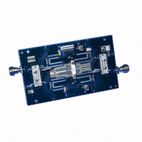
Page 8
... CGH40180PP-TB Demonstration CGH40180PP-TB Demonstration Copyright © 2009-2011 Cree, Inc. All rights reserved. The information in this document is subject to change without notice. Cree and the Cree logo are registered trademarks of Cree, Inc. 8 CGH40180PP Rev 1.1 Preliminary Schematic Amplifier Circuit Outline Amplifier Circuit Cree, Inc. ...
Page 9
... C74,C84 L10,L20 L30,L40 J1,J2 J3, CGH40180PP-TB Demonstration Copyright © 2009-2011 Cree, Inc. All rights reserved. The information in this document is subject to change without notice. Cree and the Cree logo are registered trademarks of Cree, Inc. 9 CGH40180PP Rev 1.1 Preliminary Bill of Materials Amplifier Circuit Description ...
Page 10
... Typical Package S-Parameters for CGH40180PP, Single Side (Small Signal Frequency Mag S11 Ang S11 500 MHz 0.957 -177.48 600 MHz 0.957 -178.74 700 MHz 0.957 -179.78 800 MHz 0.957 179.32 900 MHz 0.957 178.51 1.0 GHz 0.957 177.76 1.1 GHz 0.957 177 ...
Page 11
... Product Dimensions CGH40180PP (Package Type — 440199) Copyright © 2009-2011 Cree, Inc. All rights reserved. The information in this document is subject to change without notice. Cree and the Cree logo are registered trademarks of Cree, Inc. 11 CGH40180PP Rev 1.1 Preliminary Cree, Inc. 4600 Silicon Drive Durham, NC 27703 USA Tel: +1 ...
Page 12
... Copyright © 2009-2011 Cree, Inc. All rights reserved. The information in this document is subject to change without notice. Cree and the Cree logo are registered trademarks of Cree, Inc. 12 CGH40180PP Rev 1.1 Preliminary Cree, Inc. 4600 Silicon Drive Durham, NC 27703 USA Tel: +1.919.313.5300 Fax: +1 ...