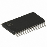
TDA5212 Infineon Technologies, TDA5212 Datasheet - Page 30

TDA5212
Manufacturer Part Number
TDA5212
Description
IC FSK/ASK RECEIVER P-TSSOP-28
Manufacturer
Infineon Technologies
Type
Receiverr
Datasheet
1.TDA5212.pdf
(49 pages)
Specifications of TDA5212
Package / Case
28-TSSOP
Frequency
902MHz ~ 928MHz
Sensitivity
-109dBm
Modulation Or Protocol
ASK, FSK
Applications
RKE, Remote Control Systems
Current - Receiving
5.4mA
Data Interface
PCB, Surface Mount
Antenna Connector
PCB, Surface Mount
Voltage - Supply
4.5 V ~ 5.5 V
Operating Temperature
-40°C ~ 85°C
Operating Frequency
928 MHz
Operating Supply Voltage
5 V
Maximum Operating Temperature
+ 85 C
Minimum Operating Temperature
- 40 C
Mounting Style
SMD/SMT
Operating Temperature (min)
-40C
Operating Temperature (max)
85C
Operating Temperature Classification
Industrial
Product Depth (mm)
4.4mm
Product Length (mm)
9.7mm
Operating Supply Voltage (min)
4.5V
Operating Supply Voltage (typ)
5V
Operating Supply Voltage (max)
5.5V
Lead Free Status / RoHS Status
Contains lead / RoHS non-compliant
Features
-
Memory Size
-
Data Rate - Maximum
-
Lead Free Status / Rohs Status
Compliant
Other names
TDA5212INTR
Available stocks
Company
Part Number
Manufacturer
Quantity
Price
Part Number:
TDA5212C3
Manufacturer:
INFINEON/英飞凌
Quantity:
20 000
TDA 5212
Applications
gain for the DC content of FSK signal remains at 200µV/kHz. The cutoff fre-
quencies of the bandpass have to be chosen such that the spectrum of the data
signal is influenced in an acceptable amount.
In case that the user data is containing long sequences of logical zeros the
effect of the drift-off of the bit slicer threshold voltage can be lowered if the offset
voltage inherent at the negative input of the slicer comparator (Pin20) is used.
The comparator has no hysteresis built in.
This offset voltage is generated by the bias current of the negative input of the
comparator (i.e. 20nA) running over the external resistor R. This voltage raises
the voltage appearing at pin 20 (e.g. 1mV with R = 100k Ω ). In order to obtain
benefit of this asymmetrical offset for the demodulation of long zeros the lower
of the two FSK frequencies should be chosen in the transmitter as the zero-
symbol frequency.
In the following figure the shape of the above mentioned bandpass is shown.
gain (pin19)
v
v-3dB
20dB/dec
-40dB/dec
3dB
0dB
f
DC
f1
f2
f3
0.18m V/kHz
2mV/k Hz
frequenzgang.WMF
Figure 4-8
Frequency characterstic in case of FSK mode
The cutoff frequencies are calculated with the following formulas:
1
=
f
⋅
Ω
1
R
330
k
π
×
2
C
+
Ω
R
330
k
Wireless Components
4 - 9
Specification, December 2006


