TDA5212 Infineon Technologies, TDA5212 Datasheet - Page 39
TDA5212
Manufacturer Part Number
TDA5212
Description
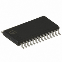
IC FSK/ASK RECEIVER P-TSSOP-28
Manufacturer
Infineon Technologies
Type
Receiverr
Datasheet
1.TDA5212.pdf
(49 pages)
Specifications of TDA5212
Package / Case
28-TSSOP
Frequency
902MHz ~ 928MHz
Sensitivity
-109dBm
Modulation Or Protocol
ASK, FSK
Applications
RKE, Remote Control Systems
Current - Receiving
5.4mA
Data Interface
PCB, Surface Mount
Antenna Connector
PCB, Surface Mount
Voltage - Supply
4.5 V ~ 5.5 V
Operating Temperature
-40°C ~ 85°C
Operating Frequency
928 MHz
Operating Supply Voltage
5 V
Maximum Operating Temperature
+ 85 C
Minimum Operating Temperature
- 40 C
Mounting Style
SMD/SMT
Operating Temperature (min)
-40C
Operating Temperature (max)
85C
Operating Temperature Classification
Industrial
Product Depth (mm)
4.4mm
Product Length (mm)
9.7mm
Operating Supply Voltage (min)
4.5V
Operating Supply Voltage (typ)
5V
Operating Supply Voltage (max)
5.5V
Lead Free Status / RoHS Status
Contains lead / RoHS non-compliant
Features
-
Memory Size
-
Data Rate - Maximum
-
Lead Free Status / Rohs Status
Compliant
Other names
TDA5212INTR
Available stocks
Company
Part Number
Manufacturer
Quantity
Price

Part Number:
TDA5212C3
Manufacturer:
INFINEON/英飞凌
Quantity:
20 000


Wireless Components
Table 5-3 AC/DC Characteristics with T
Signal Input LNI, V
Signal Input LNI, V
Signal Output LNO, V
Signal 3VOUT (PIN 24)
Signal THRES (PIN 23)
Signal TAGC (PIN 4)
MIXER
Signal Input MI/MIX (PINS 8/9)
#
3
1
2
3
1
2
3
1
2
1
2
3
4
1
2
1
2
Parameter
Voltage Gain Antenna to
IFO f
Input impedance,
f
Input level @ 1dB C. P.
f
Input 3
point f
Gain f
Output impedance,
f
Voltage Gain Antenna to
IFO f
Output voltage
Current out
Input Voltage range
LNA low gain mode
LNA high gain mode
Current in
Current out,
LNA low gain state
Current in,
LNA high gain state
Input impedance,
f
Input 3
point
RF
RF
RF
RF
= 915 MHz
= 915 MHz
= 915 MHz
= 915 MHz
RF
RF
RF
RF
rd
rd
= 915 MHz
= 915 MHz
order intercept
order intercept
= 915 MHz
= 915 MHz
THRES
THRES
THRES
= GND, low gain mode
= GND, low gain mode
= GND, low gain mode
P1dB
I
I
I
S
S
S
V
V
V
V
Symbol
IIP3
THRES_in
TAGC_out
S
TAGC_in
IIP3
I
G
G
3VOUT
11 LNA
21 LNA
22 LNA
3VOUT
THRES
THRES
THRES
11 MIX
AntMI
AntMI
LNA
MIX
LNA
A
25 °C, V
min
2.9
3.8
0
0
1
0.753 / -86.26 deg
0.912 / -30.13 deg
0.174 / 107.4 deg
0.868 / -28.1 deg
VCC
Limit Values
5 - 5
= 4.5 ... 5.5 V (continued)
-25
typ
4.2
1.5
40
19
-6
-5
3
3
5
V
V
max
3.1
4.8
50
S
S
2
-1
-1
Unit
dBm
dBm
dBm
dB
dB
µA
nA
µA
µA
V
V
V
V
Test Conditions/
Notes
f
I
see Section 4.1
or shorted to Pin 24
RSSI > V
RSSI < V
in
3Vout
Specification, December 2006
= 914 & 916MHz
= 5µA
THRES
THRES
TDA 5212
Reference
L Item
Related parts for TDA5212
Image
Part Number
Description
Manufacturer
Datasheet
Request
R

Part Number:
Description:
Manufacturer:
Infineon Technologies AG
Datasheet:
Part Number:
Description:
Manufacturer:
Infineon Technologies AG
Datasheet:
Part Number:
Description:
Manufacturer:
Infineon Technologies AG
Datasheet:
Part Number:
Description:
Manufacturer:
Infineon Technologies AG
Datasheet:
Part Number:
Description:
Manufacturer:
Infineon Technologies AG
Datasheet:
Part Number:
Description:
Manufacturer:
Infineon Technologies AG
Datasheet:
Part Number:
Description:
Manufacturer:
Infineon Technologies AG
Datasheet:
Part Number:
Description:
16-bit microcontroller with 2x2 KByte RAM
Manufacturer:
Infineon Technologies AG
Datasheet:
Part Number:
Description:
NPN silicon RF transistor
Manufacturer:
Infineon Technologies AG
Datasheet:
Part Number:
Description:
NPN silicon RF transistor
Manufacturer:
Infineon Technologies AG
Datasheet:
Part Number:
Description:
NPN silicon RF transistor
Manufacturer:
Infineon Technologies AG
Datasheet:
Part Number:
Description:
NPN silicon RF transistor
Manufacturer:
Infineon Technologies AG
Datasheet:
Part Number:
Description:
Si-MMIC-amplifier in SIEGET 25-technologie
Manufacturer:
Infineon Technologies AG
Datasheet:
Part Number:
Description:
IGBT Power Module
Manufacturer:
Infineon Technologies AG
Datasheet:
Part Number:
Description:
IC for switching-mode power supplies
Manufacturer:
Infineon Technologies AG
Datasheet: