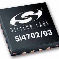
SI4702-B16-GM Silicon Laboratories Inc, SI4702-B16-GM Datasheet - Page 19

SI4702-B16-GM
Manufacturer Part Number
SI4702-B16-GM
Description
IC FM RADIO TUNER 20QFN
Manufacturer
Silicon Laboratories Inc
Datasheet
1.SI4703-B17-EVB.pdf
(46 pages)
Specifications of SI4702-B16-GM
Frequency
76MHz ~ 108MHz
Sensitivity
-99dBm
Modulation Or Protocol
FM
Applications
Cellular, MP3, PDAs, Portable Radios
Current - Receiving
18mA
Data Interface
PCB, Surface Mount
Antenna Connector
PCB, Surface Mount
Voltage - Supply
2.7 V ~ 5.5 V
Operating Temperature
-20°C ~ 85°C
Package / Case
20-QFN
Lead Free Status / RoHS Status
Lead free / RoHS Compliant
Features
-
Memory Size
-
Data Rate - Maximum
-
Lead Free Status / RoHS Status
Lead free / RoHS Compliant, Lead free / RoHS Compliant
Other names
336-1333-1
Available stocks
Company
Part Number
Manufacturer
Quantity
Price
Company:
Part Number:
SI4702-B16-GM
Manufacturer:
Silicon Labs
Quantity:
135
Part Number:
SI4702-B16-GM
Manufacturer:
SILICONIX
Quantity:
20 000
Part Number:
SI4702-B16-GMR
Manufacturer:
SILICON LABS/èٹ¯ç§‘
Quantity:
20 000
writes, starting with the upper byte of register 02h,
followed by the lower byte of register 02h, and onward
until the lower byte of the last register is reached. The
internal address counter then automatically wraps
around to the upper byte of register 00h and proceeds
from there until continuous writes end. Data transfer
ends with the STOP condition (rising edge of SDIO
while SCLK is high). After every STOP condition, the
internal address counter is reset.
For read operations, the device acknowledge is
followed by an eight bit data word shifted out on falling
SCLK edges. An internal address counter automatically
increments to allow continuous data byte reads, starting
with the upper byte of register 0Ah, followed by the
lower byte of register 0Ah, and onward until the lower
byte of the last register is reached. The internal address
counter then automatically wraps around to the upper
byte of register 00h and proceeds from there until
continuous reads cease. After each byte of data is read,
the controller IC must drive an acknowledge (SDIO = 0)
if an additional byte of data will be requested. Data
transfer ends with the STOP condition. After every
STOP condition, the internal address counter is reset.
For details on timing specifications and diagrams, refer
to
Characteristics
Control Interface Read and Write Timing Parameters,”
on page 11 and Figure 6, “2-Wire Control Interface
Read and Write Timing Diagram,” on page 11.
Table 7,
1,2,3
,” on page 10, Figure 5, “2-Wire
“2-Wire
Control
Interface
Rev. 1.1
4.9. Reset, Powerup, and Powerdown
Driving the RST pin low will disable the Si4702/03-C19
and its control bus interface, and reset the registers to
their default settings. Driving the RST pin high will bring
the device out of reset. As the device is brought out of
reset, it will sample the state of several pins to select
between 2-wire and 3-wire control interface operation,
using one of two busmode selection methods.
Busmode selection method 1 requires the use of the
GPIO3, SEN, and SDIO pins. To use this busmode
selection method, the GPIO3 and SDIO pins must be
sampled low by the device on the rising edge of RST.
The user may either drive the GPIO3 pin low externally,
or leave the pin floating. If the pin is not driven by the
user, it will be pulled low by an internal 1 M resistor
which is active only while RST is low. The user must
drive the SEN and SDIO pins externally to the proper
state.
To select 2-wire operation, the SEN pin must be
sampled high by the device on the rising edge of RST.
To select 3-wire operation, the SEN pin must be
sampled low by the device on the rising edge of RST.
Refer
(Busmode Select Method 1)
Figure 1, “Reset Timing Parameters for Busmode
Select Method 1 (GPIO3 = 0),” on page 6.
Busmode selection method 2 requires only the use of
the GPIO3 and GPIO1 pins. This is the recommended
busmode selection method when not using the internal
crystal oscillator. To use this busmode selection
method, the GPIO3 pin must be sampled high on the
rising edge of RST. The user must drive the GPIO3 pin
high externally, or pull it up with a resistor of 100 k or
less. The user must also drive the GPIO1 pin externally
to the proper state.
To select 2-wire operation, the GPIO1 pin must be
sampled high by the device on the rising edge of RST.
To select 3-wire operation, the GPIO1 pin must be
sampled low by the device on the rising edge of RST.
Refer
(Busmode Select Method 2)
Figure 2, “Reset Timing Parameters for Busmode
Select Method 2 (GPIO3 = 1),” on page 7.
Table 9 summarizes the two bus selection methods.
to
to
Table 4,
Table 5,
“Reset
“Reset
Si4702/03-C19
1,2,3
1,2,3
Timing
Timing
,” on page 6 and
,” on page 7 and
Characteristics
Characteristics
19


