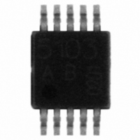
TDK5110F Infineon Technologies, TDK5110F Datasheet - Page 11

TDK5110F
Manufacturer Part Number
TDK5110F
Description
TRANSMITTER ASK/FSK SGL TSSOP10
Manufacturer
Infineon Technologies
Type
Transmitterr
Specifications of TDK5110F
Package / Case
10-TSSOP
Frequency
434MHz Center
Applications
Alarm Systems, Communication Systems
Modulation Or Protocol
ASK, FSK
Data Rate - Maximum
20 kbps
Power - Output
11dBm
Current - Transmitting
14.2mA
Data Interface
PCB, Surface Mount
Antenna Connector
PCB, Surface Mount
Voltage - Supply
2.1 V ~ 4 V
Operating Temperature
-40°C ~ 125°C
Operating Frequency
870 MHz
Operating Supply Voltage
2.5 V, 3.3 V
Maximum Operating Temperature
+ 125 C
Minimum Operating Temperature
- 40 C
Mounting Style
SMD/SMT
Lead Free Status / RoHS Status
Lead free / RoHS Compliant
Features
-
Memory Size
-
Lead Free Status / RoHS Status
Lead free / RoHS Compliant, Lead free / RoHS Compliant
Other names
SP000056180
TDK5110FXT
TDK5110FXT
Available stocks
Company
Part Number
Manufacturer
Quantity
Price
Company:
Part Number:
TDK5110F
Manufacturer:
INF
Quantity:
9 999
Company:
Part Number:
TDK5110F
Manufacturer:
INFINEON
Quantity:
616
Part Number:
TDK5110F
Manufacturer:
INFINEON/英飞凌
Quantity:
20 000
Wireless Components
8
9
10
11
12
FSKGND
CLKOUT
FSKOUT
CLKDIV
COSC
9
60 k
V
V
S
S
200 µA
6 k
1.5 k
300
+1.2 V
60 k
11
12
100 A
10
8
V
S
5 A
3 - 5
+0.8 V
Clock output to supply an external device.
An external pull-up resistor has to be added
in accordance to the driving requirements of
the external device.
A clock frequency of 3.39 MHz is selected
by a logic low at CLKDIV input (pin 9).
A clock frequency of 847.5 kHz is selected
by a logic high at CLKDIV input (pin 9).
This pin is used to select the desired clock
division rate for the CLKOUT signal.
A logic low (CLKDIV < 0.2 V) applied to this
pin selects the 3.39 MHz output signal at
CLKOUT (pin 8).
A logic high (CLKDIV open) applied to this
pin selects the 847.5 kHz output signal at
CLKOUT (pin 8).
This pin is connected to the reference oscil-
lator circuit.
The reference oscillator is working as a neg-
ative impedance converter. It presents a
negative resistance in series to an induc-
tance at the COSC pin.
This pin is connected to a switch to
FSKGND (pin 12).
The switch is closed when the signal at
FSKDTA (pin 7) is in a logic low state.
The switch is open when the signal at
FSKDTA (pin 7) is in a logic high state.
FSKOUT can switch an additional capacitor
to the reference crystal network to pull the
crystal frequency by an amount resulting in
the desired FSK frequency shift of the trans-
mitter output frequency.
Ground connection for FSK modulation out-
put FSKOUT.
Specification, October 2002
Functional Description
TDK 5110


