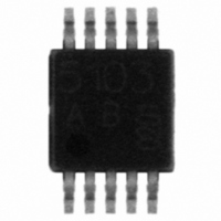
TDK5110F Infineon Technologies, TDK5110F Datasheet - Page 41

TDK5110F
Manufacturer Part Number
TDK5110F
Description
TRANSMITTER ASK/FSK SGL TSSOP10
Manufacturer
Infineon Technologies
Type
Transmitterr
Specifications of TDK5110F
Package / Case
10-TSSOP
Frequency
434MHz Center
Applications
Alarm Systems, Communication Systems
Modulation Or Protocol
ASK, FSK
Data Rate - Maximum
20 kbps
Power - Output
11dBm
Current - Transmitting
14.2mA
Data Interface
PCB, Surface Mount
Antenna Connector
PCB, Surface Mount
Voltage - Supply
2.1 V ~ 4 V
Operating Temperature
-40°C ~ 125°C
Operating Frequency
870 MHz
Operating Supply Voltage
2.5 V, 3.3 V
Maximum Operating Temperature
+ 125 C
Minimum Operating Temperature
- 40 C
Mounting Style
SMD/SMT
Lead Free Status / RoHS Status
Lead free / RoHS Compliant
Features
-
Memory Size
-
Lead Free Status / RoHS Status
Lead free / RoHS Compliant, Lead free / RoHS Compliant
Other names
SP000056180
TDK5110FXT
TDK5110FXT
Available stocks
Company
Part Number
Manufacturer
Quantity
Price
Company:
Part Number:
TDK5110F
Manufacturer:
INF
Quantity:
9 999
Company:
Part Number:
TDK5110F
Manufacturer:
INFINEON
Quantity:
616
Part Number:
TDK5110F
Manufacturer:
INFINEON/英飞凌
Quantity:
20 000
Wireless Components
Table 5-4 Supply Voltage V
Parameter
Power Amplifier Output (Pin 14)
Output Power
transformed to 50 Ohm.
V
Output Power
transformed to 50 Ohm.
V
Frequency Range Selection (Pin 15)
Transmit frequency 433 MHz
Transmit frequency 868 MHz
Input bias current FSEL
Input bias current FSEL
Crystal Frequency Selection (Pin 16)
Crystal frequency 6.78 MHz
Crystal frequency 13.56 MHz
Input bias current CSEL
Input bias current CSEL
FSEL
FSEL
1) The output-frequency range can be increased by limiting the temperature and supply voltage
2) Derating linearly to a saturation voltage of max. 140 mV at I
3) Matching circuitry as used in the 50 Ohm-Output Testboard for 434 MHz operation.
Typ. temperature dependency at 2.1 V: -0.5 dBm@-40°C and -0.5 dBm@+125°C, reference +25°C.
Typ. temperature dependency at 3.0 V: -0.3 dBm@-40°C and -1.0 dBm@+125°C, reference +25°C.
Typ. temperature dependency at 4.0 V: -0.2 dBm@-40°C and -1.5 dBm@+125°C, reference +25°C.
4) Matching circuitry as used in the 50 Ohm-Output Testboard for 868 MHz operation.
Typ. temperature dependency at 2.1 V: -0.2 dBm@-40°C and -0.7 dBm@+125°C, reference +25°C.
Typ. temperature dependency at 3.0 V: -0.5 dBm@-40°C and -1.1 dBm@+125°C, reference +25°C.
Typ. temperature dependency at 4.0 V: -0.9 dBm@-40°C and -1.0 dBm@+125°C, reference +25°C.
A smaller load impedance reduces the supply-voltage dependency.
A higher load impedance reduces the temperature dependency.
= 0 V
= V
Minimum f
Maximum f
Maximum f
range.
Tolerances of the passive elements not taken into account.
Range @ 2.1 V, +25°C: 6.5 dBm +/- 1 dBm
Range @ 3.0 V, +25°C: 10 dBm +/- 2.0 dBm
Range @ 4.0 V, +25°C: 11.5 dBm +/- 2.5 dBm
Tolerances of the passive elements not taken into account.
Range @ 2.1 V, +25°C: 7.5 dBm +/- 1.0 dBm
Range @ 3.0 V, +25°C: 10.2 dBm +/- 2.0 dBm
Range @ 4.0 V, +25°C: 11 dBm +/- 2.5 dBm
S
3)
4)
at 433 MHz
at 868 MHz
VCO
VCO
VCO
+ 1 MHz => Maximum T
+ 1 MHz => Minimum V
1 MHz => Minimum T
S
= 2.1 V ... 4.0 V, Ambient temperature T
Symbol
P
P
P
P
P
P
V
V
I
I
V
V
I
I
FSEL
FSEL
CSEL
CSEL
OUT, 433
OUT, 433
OUT, 433
OUT, 868
OUT, 868
OUT, 868
FSEL
FSEL
CSEL
CSEL
Min
7.5
5.8
7.1
7.5
-20
-25
5
7
0
0
amb
S
amb
+ 25 mV, max. + 40 MHz.
5 - 8
+ 5°C
Limit Values
5°C
11.5
10.2
Typ
6.5
7.5
10
11
amb
CLKOUT
Max
13.5
12.2
12.5
8.5
8.5
0.5
0.2
12
35
55
= -40 C ... +125 C
= 0 mA
Unit
dBm
dBm
dBm
dBm
dBm
dBm
V
V
µA
µA
V
V
µA
µA
Specification, October 2002
Test Conditions
V
V
V
V
V
V
pin open
V
V
pin open
V
V
S
S
S
S
S
S
FSEL
FSEL
CSEL
CSEL
= 2.1 V
= 3.0 V
= 4.0 V
= 2.1 V
= 3.0 V
= 4.0 V
= V
= 0 V
= V
= 0 V
TDK 5110
S
S
Reference


