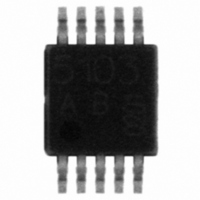
TDK5110F Infineon Technologies, TDK5110F Datasheet - Page 25

TDK5110F
Manufacturer Part Number
TDK5110F
Description
TRANSMITTER ASK/FSK SGL TSSOP10
Manufacturer
Infineon Technologies
Type
Transmitterr
Specifications of TDK5110F
Package / Case
10-TSSOP
Frequency
434MHz Center
Applications
Alarm Systems, Communication Systems
Modulation Or Protocol
ASK, FSK
Data Rate - Maximum
20 kbps
Power - Output
11dBm
Current - Transmitting
14.2mA
Data Interface
PCB, Surface Mount
Antenna Connector
PCB, Surface Mount
Voltage - Supply
2.1 V ~ 4 V
Operating Temperature
-40°C ~ 125°C
Operating Frequency
870 MHz
Operating Supply Voltage
2.5 V, 3.3 V
Maximum Operating Temperature
+ 125 C
Minimum Operating Temperature
- 40 C
Mounting Style
SMD/SMT
Lead Free Status / RoHS Status
Lead free / RoHS Compliant
Features
-
Memory Size
-
Lead Free Status / RoHS Status
Lead free / RoHS Compliant, Lead free / RoHS Compliant
Other names
SP000056180
TDK5110FXT
TDK5110FXT
Available stocks
Company
Part Number
Manufacturer
Quantity
Price
Company:
Part Number:
TDK5110F
Manufacturer:
INF
Quantity:
9 999
Company:
Part Number:
TDK5110F
Manufacturer:
INFINEON
Quantity:
616
Part Number:
TDK5110F
Manufacturer:
INFINEON/英飞凌
Quantity:
20 000
TDK5110F
Applications
Even harmonics of the signal at CLKOUT can interact with the crystal oscillator input
COSC preventing the start-up of oscillation. Care must be taken in layout by sufficient
separation of the signal lines to ensure sufficiently small coupling.
3.6
Application Hints on the Power-Amplifier
The power amplifier operates in a high efficient class C mode. This mode is
characterized by a pulsed operation of the power amplifier transistor at a current flow
θ<<π
angle of
. A frequency selective network at the amplifier output passes the
fundamental frequency component of the pulse spectrum of the collector current to the
load. The load and its resonance transformation to the collector of the power amplifier
can be generalized by the equivalent circuit of Figure 13. The tank circuit L//C//RL in
parallel to the output impedance of the transistor should be in resonance at the
operating frequency of the transmitter.
V
S
L
C
R
L
Figure 13
Equivalent power amplifier tank circuit
The optimum load at the collector of the power amplifier for “critical” operation under
idealized conditions at resonance is:
2
V
=
S
R
LC
2
*
P
O
The theoretical value of R
for an RF output power of P
= 10dBm (10mW) is:
LC
o
2
3
=
=
Ω
R
450
LC
2
*
. 0
01
“Critical” operation is characterized by the RF peak voltage swing at the collector of the
PA transistor to just reach the supply voltage V
.
S
The high degree of efficiency under “critical” operating conditions can be explained by
the low power losses at the transistor. During the conducting phase of the transistor, its
collector voltage is very small. This way the power loss of the transistor, equal to i
*u
C
CE
θ<<π.
is minimized. This is particularly true for small current flow angles of
Data Sheet
25
V 1.1, 2006-07-10


