ATAB5570 Atmel, ATAB5570 Datasheet - Page 8
ATAB5570
Manufacturer Part Number
ATAB5570
Description
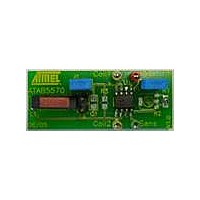
BOARD EVAL FOR ATAB5570
Manufacturer
Atmel
Type
Development kitr
Specifications of ATAB5570
Contents
Fully Assembled Evaluation Board
Product
RFID Transponders
For Use With/related Products
ATA5570
Lead Free Status / RoHS Status
Contains lead / RoHS non-compliant


5. Operating the ATA5570
5.1
5.2
5.3
8
Initialization and POR Delay
Tag-to-reader Communication
Regular-read Mode
ATA5570 [Preliminary]
The Power-On-Reset (POR) circuit remains active until an adequate voltage threshold has been
reached. This in turn triggers the default start-up delay sequence. During this configuration
period of about 192 field clocks, the ATA5570 is initialized with the configuration data stored in
EEPROM block 0. If the POR delay bit is reset, no additional delay is observed after the configu-
ration period. Tag modulation in regular-read mode will be observed about 3 ms after entering
the RF field. If the POR delay bit is set, the ATA5570 remains in a permanent damping state until
8190 internal field clocks have elapsed.
T
Any field gap occurring during this initialization phase will restart the complete sequence. After
this initialization time the ATA5570 enters regular-read mode and modulation starts automati-
cally, using the parameters defined in the configuration register.
During normal operation, the data stored within the EEPROM is cycled and the COIL1 and
COIL2 terminals are load modulated. This resistive load modulation can be detected at the
reader module.
In regular-read mode, data from the memory is transmitted serially, starting with block 1, bit 1, up
to the last block (e.g., 7), bit 32. The last block which will be read is defined by the mode param-
eter field MAXBLK in EEPROM block 0. When the data block addressed by MAXBLK has been
read, data transmission restarts with block 1, bit 1.
The user may limit the cyclic datastream in regular-read mode by setting the MAXBLK between
0 and 7 (representing each of the 8 data blocks). If set to 7, blocks 1 through 7 can be read. If set
to 1, only block 1 is transmitted continuously. If set to 0, the contents of the configuration block
(normally not transmitted) can be read. In the case of MAXBLK = 0 or 1, regular-read mode can
not be distinguished from block-read mode.
Figure 5-1.
Every time the ATA5570 enters regular- or block-read mode, the first bit transmitted is a logical
“0”. The data stream starts with block 1, bit 1, continues through MAXBLK, bit 32, and cycles
continuously if in regular-read mode.
This behavior is different from the original e555x and helps to decode PSK-modulated data.
INIT
MAXBLK = 5
MAXBLK = 2
MAXBLK = 0
= (192 + 8190
Examples of Different MAXBLK Settings
Loading block 0
Loading block 0
Loading block 0
POR delay)
0
0
0
Block 1
Block 1
Block 0
T
C
Block 4
Block 2
Block 0
67 ms;
Block 5
Block 1
Block 0
T
C
= 8 µs at 125 kHz
Block 1
Block 2
Block 0
Block 2
Block 1
Block 0
4863A–RFID–07/05
Related parts for ATAB5570
Image
Part Number
Description
Manufacturer
Datasheet
Request
R

Part Number:
Description:
DEV KIT FOR AVR/AVR32
Manufacturer:
Atmel
Datasheet:

Part Number:
Description:
INTERVAL AND WIPE/WASH WIPER CONTROL IC WITH DELAY
Manufacturer:
ATMEL Corporation
Datasheet:
Part Number:
Description:
Low-Voltage Voice-Switched IC for Hands-Free Operation
Manufacturer:
ATMEL Corporation
Datasheet:
Part Number:
Description:
MONOLITHIC INTEGRATED FEATUREPHONE CIRCUIT
Manufacturer:
ATMEL Corporation
Datasheet:
Part Number:
Description:
AM-FM Receiver IC U4255BM-M
Manufacturer:
ATMEL Corporation
Datasheet:
Part Number:
Description:
Monolithic Integrated Feature Phone Circuit
Manufacturer:
ATMEL Corporation
Datasheet:
Part Number:
Description:
Multistandard Video-IF and Quasi Parallel Sound Processing
Manufacturer:
ATMEL Corporation
Datasheet:
Part Number:
Description:
High-performance EE PLD
Manufacturer:
ATMEL Corporation
Datasheet:
Part Number:
Description:
8-bit Flash Microcontroller
Manufacturer:
ATMEL Corporation
Datasheet:
Part Number:
Description:
2-Wire Serial EEPROM
Manufacturer:
ATMEL Corporation
Datasheet: